Power Component in PCB card Layout can greatly help to decrease the noise, proper arrangement for MOSFET and capacitors (input, sidewalk and output) are important.
as we all know that the current waveform at the top and bottom power switches is a pulse with a very high δI/δt. Therefore, the path connecting the switches should be as short as possible to minimize the noise picked up by the controller and the noise transmitted by the inductive loop.
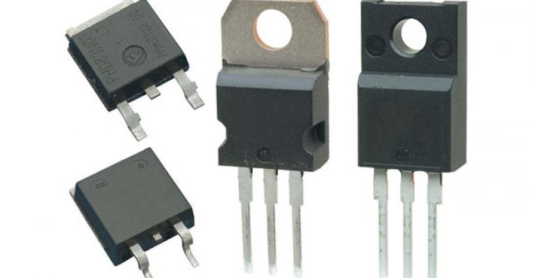
When using a pair of DPAK or SO-8 packaged FETs on one side of the PCB, it is best to rotate the two FETs in opposite directions so that the switch nodes are on one side of the pair of FETs and use the appropriate ceramic bypass capacitors to the high side.

DPAK or SO-8 packaged FETs
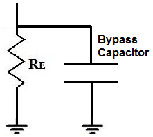
Leakage current is bypassed to the low side source. Be sure to place the bypass capacitor as close as possible to the MOSFET (see below Figure) to minimize the inductance around the loop through the FET and capacitor.

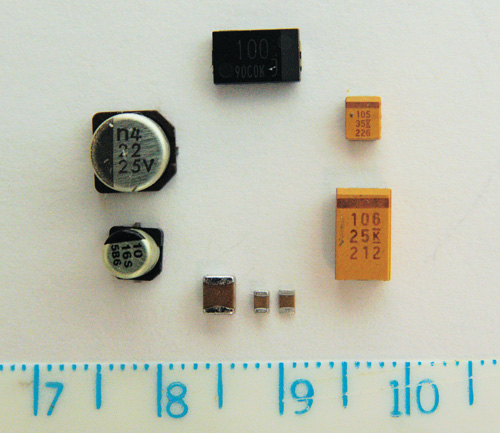
The placement of the input bypass capacitor and the input bulk capacitor is critical to controlling ground bounce. The negative terminal connection of the output filter capacitor should be as close as possible to the source of the low-side MOSFET, which helps to reduce the loop inductance that causes ground bounce. Cb1 and Cb2 in below Figure are ceramic bypass capacitors. The recommended values for these capacitors range from 1 μF to 22 μF. For high current applications, a larger value of the filter capacitor should be connected in parallel, as shown by CIN in Figure 2.

Thermal considerations and ground plane
Under heavy load conditions, the equivalent series resistance (ESR) of power MOSFETs, inductors, and bulk capacitors generates a large amount of heat. For efficient heat dissipation, the example of Figure 2 places a large area of copper beneath these power devices.
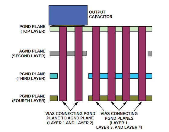
The heat dissipation effect of the multilayer PCB is better than that of the 2-layer PCB. To improve heat dissipation and electrical conductivity, 2 ounces of copper should be used on a standard 1 ounce copper layer. It is also helpful to have multiple PGND layers connected together via vias. Figure 3 shows the PGND layer on the top, third, and fourth layers of a 4-layer PCB design.


