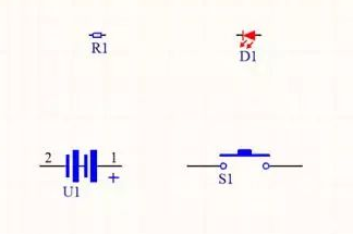
After the completion of component package drawing on the schematic, you can start draw the PCB Schematic Electrical Connection. First we put the components we need to use in the schematic.

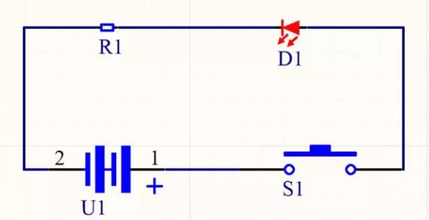
Then place a wire with electrical properties to connect the components, and a packaged schematic is complete. The connection on the schematic is the connection of the actual circuit.

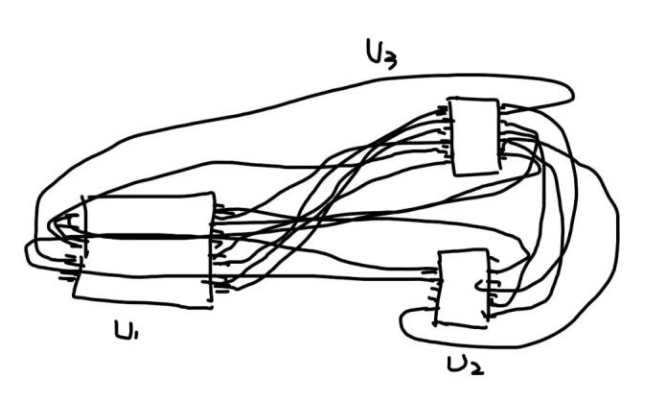
Sometimes, the distance between the two chips in the schematic is relatively long. If the line is connected to two pins, it may be necessary to draw a long and curved line. It is very troublesome to draw, and affect the visual performance of PCB schematic diagram probably like the below Figure:

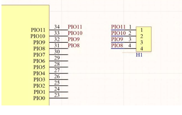
At this point, we need another way to represent the PCB Schematic Electrical Connection – the network label (Net Label), the network label can replace the part of the pin connected by wire. For a instant, the following figure is a pin that connects two chips directly with wires:

Two identical network labels indicate the connection of two pins. Although no electrical wire connections are made, the tool software considers the two pins to be on the same electrical network. When draw the PCB schematic, we can choose the place wire or network label according to the actual situation.
It should be noted that the connection and network label are mainly used in the project of single schematic. For the engineering of multiple drawings (the schematic is too big to be drawn on a piece of paper) which is quite commonly see when reverse engineering Multilayer PCB Board, we also need to use the port. Network identifiers such as (port), Sheet Entry, and Off-sheet Connector, which describe the connection between multiple drawings.


