PCB Reverse Engineering Extended Services
PCB Reverse Engineering except has the concept of PCB Cloning, it has also included some of the other concepts and extended service categories such as Microcontroller Cracking, reverse compiling of PCB Board schematic diagram, preparation of BOM list, as well as PCB design and other technical concepts.
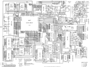
Backward Engineering Printed Circuit Board Schematic Diagram
The schematic diagram is a drawing composed of electrical symbols to analyze the circuit principle. It has an integral role in product debugging, maintenance and improvement. Schematic backward engineering Printed Circuit Board Schematic Diagram is in contrary with forward design. The forward design is started from the schematic design or scratch, and then proceed with PCB design and layout according to the schematic diagram.
The backward engineering schematic diagram of PCB Board refers to the reverse derivative of the product based on the existing PCB layout drawing/gerber file or PCB physical object. The purpose of schematic diagram is for the sake of facilitating the technical analysis of the product and to assist the product prototype debugging or upgrade in the upcoming steps.

backward engineering PCB schematic
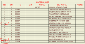
BOM list preparation
In the process of product reverse technology research and imitation development, the preparation of the BOM list, the component orientation map of Surface mount assembly, and the SMT component placement coordinate diagram are all necessary documentations for prototype assembly, SMT component assembly, final prototype design and assembly production.
BOM (bill of materials) is the basis for procurement of electronic/mechanical components, it records the various components, modules and other special materials required for electronic product assembly. The most important thing in the preparation of the BOM list is the requirement of accurate measurement values upon various parameters on the components, because if the parameters of the components are wrong or inaccurate, it may affect the judgment of the device and the accuracy of material procurement, and may even result in the project development failure in the process of prototype development and finally directly lead to the PCB Reverse Engineering Failure.

PCB BOM bill of material from PCB Reverse engineering
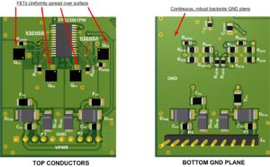
Modify PCB Layout
Modify PCB layout is the related concept or extended service for PCB Reverse Engineering, it refers to the circuitry pattern modification or re-layout/re-track on the extracted PCB Layout documentations which obtained from physical PCB board, which will be able to realize the functionality modification on original Printed circuit board, it can help to upgrade the product swiftly and satisfy the customer’s personalization and special customized expectation.

pcb layout or gerber file modification


