
Designing a Printed Circuit Board (PCB) is a meticulous process that requires precision and careful planning to ensure signal integrity, efficient component placement, and manufacturability. Whether designing from scratch or reverse engineering an existing PCB board, following structured design procedures is essential.

Baskılı Devre Kartı (PCB) tasarlamak, sinyal bütünlüğünü, etkili bileşen yerleşimini ve üretilebilirliği garantilemek için hassasiyet ve dikkatli planlama gerektiren titiz bir süreçtir. Sıfırdan tasarım yapmak veya mevcut bir PCB kartını tersine mühendislik yapmak olsun, yapılandırılmış tasarım prosedürlerini takip etmek esastır.
1. Schematic Design and Netlist Generation
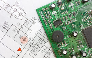
The first step in PCB design is using a schematic design tool to create a logical representation of the circuit. This schematic includes all electronic components, their interconnections, and signal paths. Once the schematic is complete, a netlist is generated, which serves as a connectivity map between components.
However, in special cases, such as simple PCB boards, it may not be necessary to create a full schematic if a netlist already exists. In such situations, designers can bypass the schematic step and manually input the netlist directly into the PCB layout software. The system allows users to assign component footprints manually, ensuring a functional board layout.
2. Netlist Modification and Component Footprint Assignment
Once the netlist is generated, designers may need to manually modify it to optimize component placement and connectivity. This involves defining fixed pins on specific components that have already been designed on the soldering pads in the schematic diagram. Proper pin definition is crucial for ensuring accurate signal flow and grounding strategies.
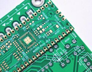
For unused pins or those without direct connections, they can be assigned to ground (GND), protection ground, or other reference voltages to maintain circuit stability. Designers must also categorize pins properly and ensure that names in the schematic diagram match those in the PCB layout. Special attention must be given to diodes, transistors, and other semiconductor components, ensuring that their footprints align correctly with the PCB library.
Depois que a netlist é gerada, os designers podem precisar modificá-la manualmente para otimizar o posicionamento e a conectividade dos componentes. Isso envolve definir pinos fixos em componentes específicos que já foram projetados nas almofadas de solda no diagrama esquemático. A definição adequada dos pinos é crucial para garantir o fluxo preciso do sinal e estratégias de aterramento.
Para pinos não utilizados ou aqueles sem conexões diretas, eles podem ser atribuídos ao aterramento (GND), aterramento de proteção ou outras tensões de referência para manter a estabilidade do circuito. Os designers também devem categorizar os pinos corretamente e garantir que os nomes no diagrama esquemático correspondam aos do layout do PCB. Atenção especial deve ser dada a diodos, transistores e outros componentes semicondutores, garantindo que suas pegadas se alinhem corretamente com a biblioteca do PCB.
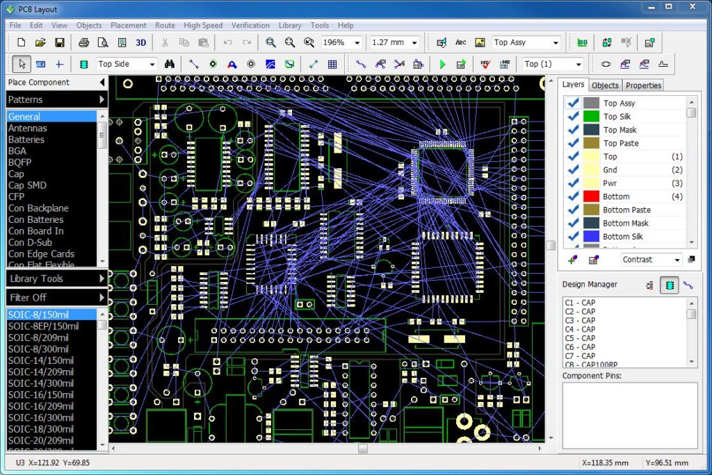
3. PCB Layout and Reverse Engineering Considerations
During the PCB layout process, components are arranged on the board to optimize electrical performance, heat dissipation, and manufacturability. High-speed signals, power traces, and sensitive analog circuits should be carefully routed to minimize noise, crosstalk, and signal integrity issues.
For PCB reverse engineering, analyzing the original PCB layout, Gerber files, and BOM lists is essential. Engineers must carefully reconstruct the schematic diagram, netlist, and component footprints to ensure the new board functions identically to the original. If documentation is missing, reverse engineering techniques such as scanning layer traces, measuring impedance, and extracting netlists from the physical PCB are used.
В процессе компоновки печатной платы компоненты размещаются на плате для оптимизации электрических характеристик, рассеивания тепла и технологичности. Высокоскоростные сигналы, силовые трассы и чувствительные аналоговые схемы должны быть тщательно проложены, чтобы минимизировать шум, перекрестные помехи и проблемы целостности сигнала.
Для обратного проектирования печатных плат необходим анализ исходной компоновки печатной платы, файлов Gerber и списков BOM. Инженеры должны тщательно реконструировать принципиальную схему, список соединений и посадочные места компонентов, чтобы гарантировать, что новая плата функционирует идентично оригиналу. Если документация отсутствует, используются методы обратного проектирования, такие как сканирование трасс слоев, измерение импеданса и извлечение списков соединений из физической печатной платы.
Conclusion
Whether designing a PCB from scratch or cloning/reproducing an existing board, following a structured design approach ensures functionality and reliability. Schematic creation, netlist management, and footprint assignment are critical steps that directly impact PCB layout, manufacturing, and reverse engineering processes. By carefully modifying the netlist and ensuring component alignment, designers can create high-performance, manufacturable PCBs that meet both functional and industrial requirements.

use la herramienta de diseño esquemático para dibujarlo y luego genere la lista de red correspondiente, por supuesto, en circunstancias especiales, como una placa de PCB simple, no es necesario realizar el diseño de dibujo esquemático si la lista de redes ha existido, ingrese directamente en el sistema de diseño de PCB, en el sistema puede recoger la huella del componente directamente para generar la lista de red manualmente


