Today we will continue to introduce the function in Altium Designer’s preference: PCB default settings.
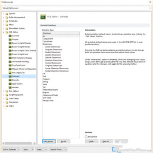
we can first enter preference>>PCB>>defaults to set the default values of the PCB, so that the PCB design drawing environment is more in line with personal habits and actual operations Demand in order to achieve more efficient goals and effects.

Function hidden in preference of Altium Designer—PCB default settings
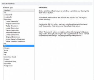
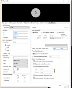
As shown in above Figure 1, this tab is specifically used to set the PCB default values. Here you can set the functions that may be used in PCB board route layout drawing cloning, such as pads, copper, characters, line segments, vias, etc. Double-click the corresponding option that needs to be set by default. At this time, a new dialog box will pop up, and you can set the corresponding settings in this new dialog box. Examples are shown in Figures 2 and 3:


If you are in a team collaboration to reverse engineering PCB board, it is best to maintain team consistency at this time, then you can export this default setting to your friends, so that you can work together in a unified manner.
Let’s introduce the method of import and export
See the position in Figure 4. When you complete the default settings, click “save as” in the red box in the figure to save. The default settings are exported and saved on your computer.
Many functions already exist in preferences, we only need to perform simple check operations to use them very conveniently. Again, there are so many good functions, and what is missing is that everyone does not understand. So looking at the very simple functions, I wrote an article to give you a general announcement, I hope you can use these things to make your design more convenient and efficient! !


