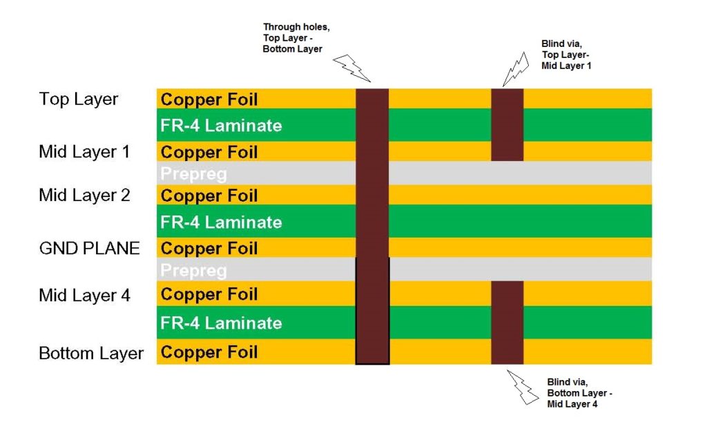
Since the invention of the PCB by the Austrian engineer Paul Eisler in 1936 and its use in radio circuits, the PCB has been widely accepted and rapidly developed by the electronics industry. Originally, PCB Circuit Board Structure was single-sided, and later developed to double-sided, then four layers, and now it has grown to multiple layers. In general, the structure of the PCB circuit board is becoming more and more complex.

The number of layers (conductive layers) of the PCB circuit board is generally even, which is determined by the level of the process in the printed circuit board manufacturing. The odd-numbered PCBs are prone to one-sided tilting during the lamination of the production process, which is not conducive to the soldering of surface mount components (SMD).
According to the IPC-A-600 standard issued by the International Electronics Industry Association (IPC), the PCB BOW and Twist height must not exceed 0.75% of its diagonal length. Due to the symmetry of the PCB Circuit Board Structure of the even-numbered layers of PCBs, it is less prone to warp at the press-fit. Therefore, designing the number of layers of the PCB to an even number has become the industry’s default convention.


