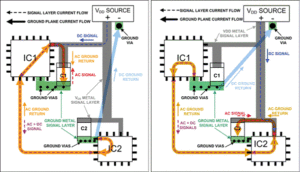
Successful Grounding in PCB Card Reverse Engineering
In below article we discuss PCB grounding. This is undoubtedly one of the most difficult subjects in PCB Card reverse engineering. While the basic concepts are relatively simple, implementation is very involved.
For linear systems the ground is the reference against which we base our signal. Unfortunately, it has also become the return path for the power supply current in unipolar supply systems. Improper application of grounding strategies can destroy high accuracy
linear system performance.
Grounding is an issue for all analog designs and it can be said that implementing a PCB based circuit doesn’t change the fact that proper implementation is essential. Fortunately, certain principles of quality grounding, namely the use of ground planes, are intrinsic to the PCB environment.

successful grounding in PCB card reverse engineering
This factor is one of the more significant advantages to PCB based analog designs and reverse engineering, and appreciable discussion of this section is focused on this issue.
Some other aspects of grounding that must be managed include the control of spurious ground and signal return voltages that can degrade performance. These voltages can be due to external signal coupling, common currents, or simply excessive IR drops in
ground conductors.
Proper conductor routing and sizing, as well as differential signal handling and ground isolation techniques enable control of such parasitic voltages. One final area of grounding to be discussed is grounding appropriate for a mixed-signal, analog/digital environment. Indeed, the single issue of quality grounding can influence the entire layout philosophy of a high performance mixed signal PCB design—as it well should.


