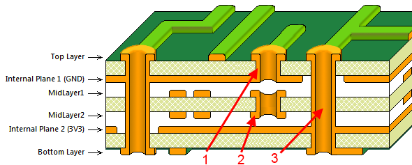
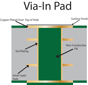
Via is one of the important components of a multi-layer PCB. The cost of drilling is usually 30% to 40% of the cost of PCB board manufacturing. From the perspective of PCB Board Via Designing , a via is mainly composed of two parts, one is a drill hole among the different layers, and the other is a pad area around the hole.

The size of the two parts determines the size of the hole. Obviously, in high-speed, high-density PCB design, the designer always hopes that the smaller the via, the better, so that more wiring space can be left on the board to ease the process of PCB wiring layout and component arrangement.
In addition, the smaller the via, the parasitic capacitance of its own. The smaller the vias is, the more suitable it is for high-speed circuits. However, the reduction in the size of the hole also brings about an increase in cost, and the size of the via hole cannot be reduced indefinitely. It is limited by the process techniques such as drilling and plating: the smaller the hole, the smaller the drill bits it will need to use and the longer time the hole drilling going to take, and it is easier to deviate from the center position and misregistration will happen which could damage the subsequent process; and when the depth of the hole exceeds 6 times the diameter of the hole, there is no guarantee that the hole wall can be uniformly deposited with copper.


