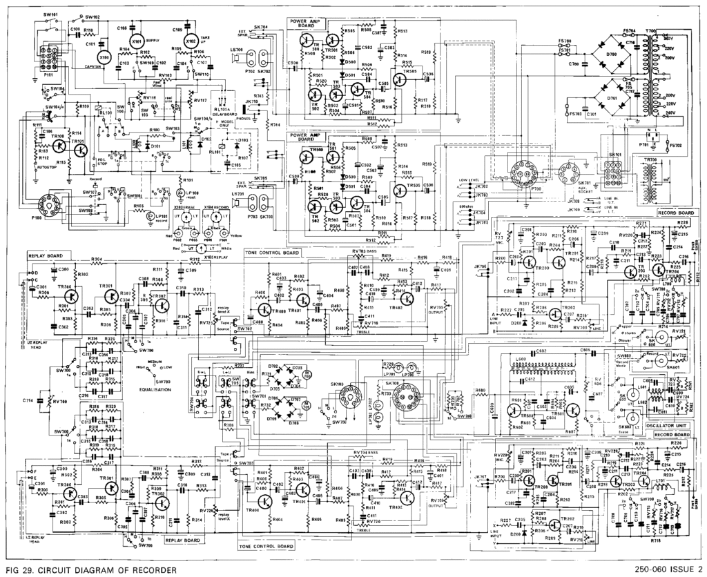
Engineer needs to execute PCB Board schematic diagram inspection, which refers to the below aspects:
1, Low speed interface;
2, Integrated Circuit;
3, Schematic diagram comment;
4, Newly designed unit circuit schematic;
5, I/O
1st is Low Speed Interface,
Whether the I2C/SMB interface has a pull-up resistor, the slave address is the same, and the address can be set with the pull-down resistor.
Enable the signal with the correct pull-up resistor (such as SPI CS#)
Undetermined level signal, MARK address needs to design pull-down resistor
Reset signal has reset chip
Signal that needs level shifting, chip switching setting direction is correct
2nd is about the Integrated Circuit:
Is there an Integrated Circuit or Transistor that has been discontinued?
Is there an Integrated Circuit or Transistor that is difficult to purchase?
Is there an Integrated Circuit or Transistor with a long procurement cycle?
Whether the device can reduce costs when implementing the same function.

3rd is concerning the schematic comment and unit circuitry schematic:
Does the homepage have a frame map?
Test point signal to be marked
Is there a comment on the GND test point?
Whether the necessary parts have the necessary comments
Whether the PIN is one-to-one, especially the connector, the package that you draw by engineer
Are there any special requirements for the window opening and process of production that are reflected on the schematic when restore it from physical PCB Board?
Is the input/output property of all PINs in the schematic symbol and the Datasheet
Is the device (resistance) that is not soldered correctly labeled with resistance, and is it reflected on the schematic?
The function of the unit circuit design, whether the designer has an unclear place
4th is for the external interface:
Are you carefully checking the interface signals of the carrier/subboard/backplane to ensure one-to-one correspondence which is also critical in the process of PCB Reverse engineering (labeling the position in the PCB)?
Is the JTAG signal level correct?
Is the JTAG daisy chain properly connected, does it take into account the compatibility of only one chip?
Whether the high-speed signal of the external interface, TX/RX carefully confirms which side is used as a reference
Whether the connector interferes with the structure during the selection.


