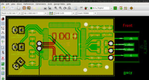
In the PCB Board Reverse Engineering, Circuitry Layout is an important step to complete the product design. It can be said that the previous preparation work is done for it. In the whole PCB board, the circuitry design process is the highest, the trick is the finest, and the workload is the largest. The PCB layout has single-sided layer, double-sided layer, and multi-layer layout. There are two ways to route: automatic routing and interactive routing.
Before automatic routing, you can use interactive pre-wired lines that require more stringent requirements. The edges of the input and output should avoid adjacent parallel to avoid reflection interference. If necessary, ground wire should be isolated. The wiring of two adjacent layers should be perpendicular to each other, and parasitic coupling is easy to occur in parallel.

PCB Board Reverse Engineering Procedures
The routing rate of automatic routing depends on a good layout, and the wiring rules can be preset, including the number of bending of the traces, the number of vias, the number of steps, and the like. Generally, the exploration type warp line is firstly connected, and the short lines are quickly connected, and then the labyrinth wiring is performed. First, the wiring to be cloth is optimized for the global routing path, and the laid line can be disconnected as needed. And try to re-route to improve the overall effect.
For the current high-density PCB board reverse engineering, it has been felt that the through-hole is not well adapted. It wastes a lot of valuable wiring channels. To solve this contradiction, blind hole and buried hole technology have emerged, which not only completes the function of the via hole. It also saves a lot of wiring channels to make the wiring process more convenient, smoother and more perfect. The PCB board reverse engineering procedure is a complicated and simple process. To master it well, it also needs extensive electronic engineering design. When people go to their own experience, they can get the truth.


