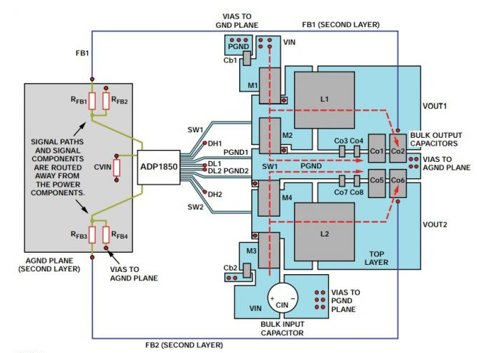
PCB board physical planning is very important, the current loop area must be minimized, and the power supply components must be arranged so that the current flows smoothly, avoiding sharp corners and narrow paths. This will help reduce parasitic capacitance and inductance, eliminating ground bounce.
Below Figure shows the PCB board layout of a dual output buck converter using the switch controller ADP1850. Note that the layout of the power device minimizes current loop area and parasitic inductance. The dashed line indicates the high current path. This physical planning technique can be used by both synchronous and asynchronous controllers. In asynchronous controller designs, Schottky diodes replace low-side switches.


