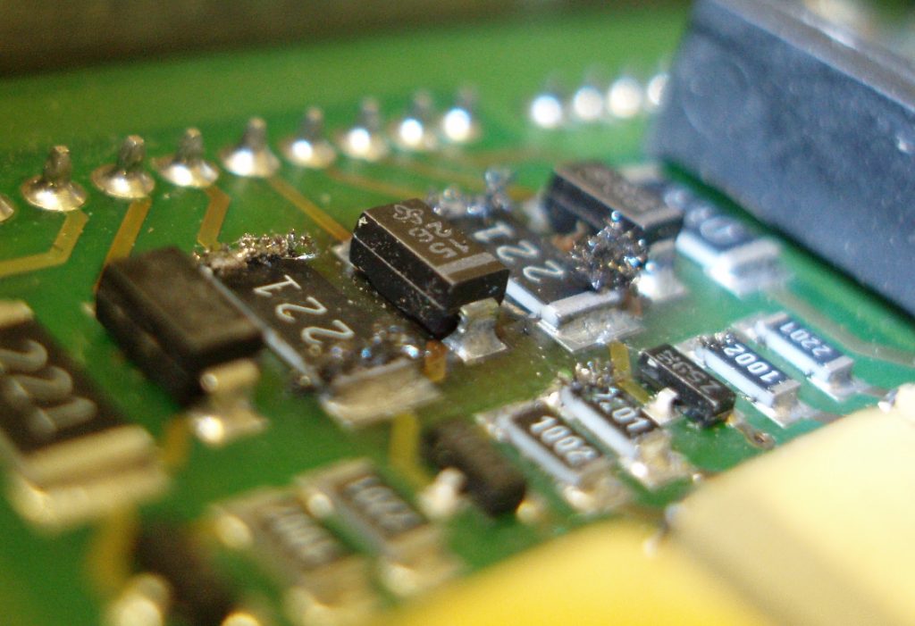
In addition to the conductive layer and the dielectric layer, the laminated structure of the PCB further includes a solder resist layer and a silk screen layer which are PCB Board Layer Composition. The solder mask covers the surface signal layer (top layer and bottom layer) of the PCB and is mainly composed of a solder mask, in the previous articles we have introduced how to judge quality of pcb solder resist mask;
Anti-welding paint is insulated, commonly known as solder mask, the most commonly used color of the solder mask is green, but also blue, red, white, black and other colors. Like the planar layer, the solder mask is also a “negative film.” Because by default, the surface of the PCB should be covered with solder mask, only areas that require soldering or need to be in contact with other conductors (such as shielded frames) require “ink windowing or solder mask opening.”
In the PCB design procedures, it is usually not necessary to pay too much attention to the solder mask, because most PCB-aided design software (such as Cadence allegro, Altium Designer) will automatically give each pad a solder mask according to a set of editable rules. Plan a “window or opening” that is typically slightly larger than the actual area of the soldering pad.
The main role of the solder mask is to prevent adjacent conductors from shorting during soldering, as shown in below Figure. The silkscreen layer of the PCB consists mainly of text and patterns, located above the solder mask and the outermost layer of the PCB. Its role is to mark the outer contour, bit number and polarity point of the component.


