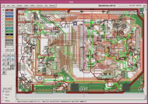
How to deal with some theoretical conflicts in actual PCB Board Gerber File Cloning:
1. Basically, it is right to separate the analog/digital division to fit for the PCB board design requirement. It should be noted that the signal trace should not cross the moat, and the return current path of the power supply and the signal should not become too large.

How to deal with some theoretical conflicts in actual PCB Board Gerber File Cloning:
2. The crystal oscillator is an analog positive feedback oscillation circuit. To have a stable oscillation signal, it must meet the loop gain and phase specifications. The oscillation specifications of the analog signal are very susceptible to interference. Even with the addition of ground guard traces, the interference may not be completely isolated. And too far away, the noise on the ground plane will also affect the positive feedback oscillation circuit. Therefore, the distance between the crystal and the chip must be close in the PCB board design rule checking.
3. Indeed, there are many conflicts between high-speed PCB design layout wiring and EMI requirements. But the basic principle is that the resistance, capacitance, or ferritebead added by EMI cannot cause some electrical characteristics of the signal to fail to meet the specifications. Therefore, it is best to first use the arrangement of wiring and PCB stacking techniques to solve or reduce EMI problems, such as high-speed signals to the inner layer. Finally, the resistance capacitor or ferrite bead is used to reduce the damage to the signal.


