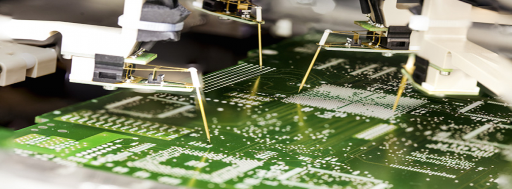
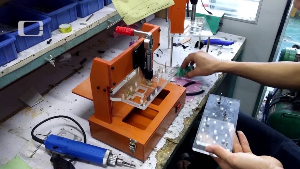
PCB Board Copying Gerber File extracted from the physical PCB sample through reverse engineering technique needs to be test through composite testing, and a composite tester is an instrument that integrates online and functional tests into one system. The PCB after manufactured is first tested online through a needle bed, and then the PCB is functionally tested with a boundary connector.

The basic principle of the PCB gerber file tester using this method to judge the fault is: firstly, based on a fault-free PCB, according to the pre-designed operation steps, a set of test data of the PCB is established, and then can be used for the same production batch ( The PCB with the same circuit topology and the same component position is basically faulty.
Since the PCB tester can establish the required basic data by measuring the “OK PCB board”, it can be analyzed without the schematic diagram when the identical “NG PCB board” is repaired. More advanced PCB testers can generate network tables in a common format that can be exported and imported into other EDA software.
Various testers are also flawed. Limited electrical contact has begun to become one of the biggest technical challenges in online testing. The components used on the PCB are getting smaller and smaller, and the pins and traces are getting denser. These factors make the density of components and circuits on the PCB higher and higher, which increases the difficulty of electrical contact and reduces the coverage of test node.

In addition, PCBs tend to be smaller and denser. This makes the additional test nodes on the PCB have no effect on the value added of the final product, so the design of the test nodes on the PCB is gradually reduced, which also makes the electrical contact during testing more difficult. Another challenge facing electrical testing comes from VHF circuits. When the frequency exceeds 1 GHz, even if electrical contact is possible, some of the parameter values of the component will become very small at very high frequencies, which is very difficult to measure. The test node itself becomes a small transmitting antenna at very high frequencies, affecting the measurement, so designers are less willing to use electrical testing, and prefer to use X-ray systems and optical inspection systems for defect and fault testing.


