PCB Board Component Layout Cloning is a critical step for printed circuit board reverse engineering, since it will refer the arrangement of each electronic/mechanical locations on the board which can greatly affect the performance of electronic appliance;

PCB Board Component Layout Cloning is for PCB reverse engineering
Since manual pcb board layout is used, the first step is to place the components and parts on the PCB board. Separate noise-sensitive components and noise-producing components. There are two criteria for accomplishing this task:
1. Divide the Component in the circuit schematic into two categories: high-speed (>40MHz) devices and low-speed devices. If possible, place high-speed components as close as possible to the circuit board’s connectors and power supply.
2. Divide the above categories into three sub-categories: pure digital, pure analog and mixed signal. Place the digital devices as close as possible to the connectors and power supply of the board.
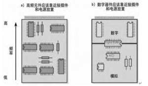
The relayout strategy of electronic PCB card should conform to the PCB card component layout shown in below Figure.

In circuits with accuracy higher than 12 bits, the placement of active components on the PCB is very important. Place high-frequency components and digital devices as close as possible to the connectors
Pay attention to the relationship between high-speed devices, low-speed devices, circuit board connectors and power supply. In Figure 2b, the digital device is closest to the connector and power supply of the circuit board, separated from other digital and analog circuits. Purely analog devices are the furthest away from digital devices to ensure that switching noise does not couple into the analog signal path.


