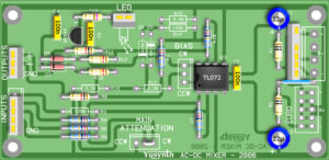
The main parasitic components generated by circuit board wiring are resistance, capacitance and inductance. In the process of the PCB Board Circuit Diagram Reverse Engineering , all parasitic components have the opportunity to interfere with the circuit performance. When a system mixes digital and analog components, careful reverse engineering PCB card is the key to the success of the circuit board.

Parasitic Components in PCB Board Circuit Diagram Reverse Engineering
In particular, digital traces wiring that are close to high-impedance analog traces that often change will cause severe coupling noise. This phenomenon can only be avoided by keeping these two traces at a distance. This article quantifies the most difficult circuit board parasitic components, circuit board capacitance, and lists examples of clearly visible circuit board performance.
Unnecessary capacitors cause trouble, two adjacent parallel traces will form wiring capacitance.
Note: Arranging two traces adjacent to each other can form a capacitor on a circuit board. Because of this kind of capacitance, a fast voltage change on one line can cause a current signal on a slow voltage on the other line. When high-impedance analog traces are close to digital traces, this type of capacitance may cause problems in sensitive mixed-signal circuits.
Note: A 16-bit digital-to-analog converter with an output voltage of 65536 steps composed of three 8-bit digital potentiometers and three operational amplifiers. If VDD is 5V in this system, the resolution or LSB size of this digital-to-analog converter is 76.3μV.


