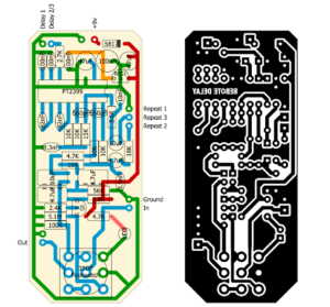
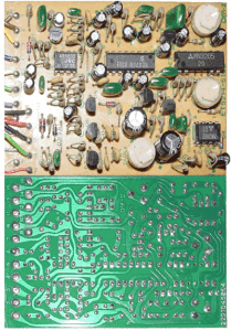
Under normal circumstances, Multilayer Printed Circuit Board Schematic Reverse Design is carried out according to circuit functions. When re-wiring on the PCB board’s outer layer, more circuitry wiring pattern is required on the soldering surface and less wiring on the component surface, which is more convenience to the maintenance and troubleshooting of the printed circuit board.

Multilayer Printed Circuit Board Schematic Reverse Design is carried out according to circuit functions. When re-wiring on the PCB board’s outer layer, more circuitry wiring pattern is required on the soldering surface and less wiring on the component surface
Thin, dense wires and signal wires that are susceptible to interference are usually reversed designed in the inner layer. A large area of copper foil should be more evenly distributed in the inner and outer layers, which will help reduce the warpage of the PCB board and also enable a more uniform coating on the surface during electroplating.
In order to prevent the shape processing from damaging the printed wires and causing inter-layer shorts/opening during mechanical processing, the distance between the conductive pattern of the inner and outer layer wiring area and the edge of the board should be greater than 50mil when reverse design Multilayer Printed Circuit Board Schematic.

the distance between the conductive pattern of the inner and outer layer wiring area and the edge of the board should be greater than 50mil when reverse design Multilayer Printed Circuit Board Schematic
Multilayer PC board wiring should separate the power layer, ground layer and signal layer to reduce interference between power, ground and signals. The lines of two adjacent layers of printed circuit boards should be as perpendicular to each other as possible, or follow diagonal lines or curves, and not parallel lines to reduce the coupling and interference between the substrate layers. And the wire should be as short as possible, especially for small signal circuits, the shorter the wire, the smaller the resistance, and the smaller the interference.


