
Multilayer HDI PCB Board Applications
Multilayer High-Density Interconnect (HDI) PCB boards have become a core technology in modern electronics, enabling high-performance, compact, and reliable devices across a wide range of industries. HDI PCBs differ from conventional boards by featuring finer lines, smaller vias (such as microvias, blind vias, and buried vias), higher layer counts, and higher wiring density per unit area. This advanced structure allows engineers to design complex, high-speed circuits in significantly smaller footprints.
Las placas PCB de interconexión de alta densidad (HDI) multicapa se han convertido en una tecnología esencial en la electrónica moderna, permitiendo dispositivos de alto rendimiento, compactos y fiables en una amplia gama de industrias. Las PCB HDI se diferencian de las placas convencionales por sus líneas más finas, vías más pequeñas (como microvías, vías ciegas y vías enterradas), mayor número de capas y mayor densidad de cableado por unidad de área. Esta estructura avanzada permite a los ingenieros diseñar circuitos complejos de alta velocidad en un tamaño significativamente menor.
Applications in Consumer Electronics
One of the most widespread uses of multilayer HDI PCBs is in consumer electronics, where miniaturization and performance are crucial. Smartphones, tablets, and wearable devices rely on HDI boards to accommodate powerful processors, large memory modules, and multi-band communication systems within thin, compact enclosures. The use of stacked vias and laser-drilled microvias in HDI PCBs allows manufacturers to integrate multiple functions on a single compact board, improving efficiency while reducing weight and size.
Applications in Automotive and Industrial Control Systems
In automotive electronics, HDI PCBs are used for advanced driver-assistance systems (ADAS), engine control units (ECUs), infotainment systems, and electric vehicle (EV) battery management systems. These applications demand high reliability, heat resistance, and EMI shielding, all of which HDI technology supports through careful layer stack design and impedance control.
Similarly, industrial control systems, such as programmable logic controllers (PLCs), rely on multilayer HDI PCBs for real-time data processing, sensor integration, and communication protocols in automation environments. HDI’s ability to support mixed-signal designs makes it ideal for these settings.
Otomotiv elektroniğinde, HDI PCB’ler gelişmiş sürücü destek sistemleri (ADAS), motor kontrol üniteleri (ECU’lar), bilgi-eğlence sistemleri ve elektrikli araç (EV) pil yönetim sistemleri için kullanılır. Bu uygulamalar yüksek güvenilirlik, ısı direnci ve EMI koruması gerektirir ve bunların hepsi HDI teknolojisinin dikkatli katman yığını tasarımı ve empedans kontrolü aracılığıyla desteklediği şeylerdir.
Benzer şekilde, programlanabilir mantık denetleyicileri (PLC’ler) gibi endüstriyel kontrol sistemleri otomasyon ortamlarında gerçek zamanlı veri işleme, sensör entegrasyonu ve iletişim protokolleri için çok katmanlı HDI PCB’lere güvenir. HDI’nin karışık sinyal tasarımlarını destekleme yeteneği onu bu ayarlar için ideal hale getirir.
Applications in Aerospace, Medical, and Military Equipment
In sectors like aerospace, medical, and defense, the demand for performance, reliability, and miniaturization is even more stringent. HDI PCBs are widely used in satellite communication modules, implantable medical devices, avionics systems, and tactical military equipment. These boards are designed to withstand extreme temperatures, vibrations, and radiation, often featuring 10+ layers with buried and stacked microvias.
Key Advantages in Application
Across all industries, multilayer HDI PCBs offer significant advantages, including:
-
Higher circuit density and signal routing flexibility
-
Improved electrical performance for high-speed and high-frequency applications
-
Compact form factors for miniaturized devices
-
Better thermal management and EMI control
As electronic products continue to evolve toward smarter, faster, and smaller solutions, Multilayer HDI PCB boards will remain an essential backbone in enabling next-generation innovations.
W sektorach takich jak lotnictwo, medycyna i obronność zapotrzebowanie na wydajność, niezawodność i miniaturyzację jest jeszcze bardziej rygorystyczne. Płytki PCB HDI są szeroko stosowane w modułach komunikacji satelitarnej, wszczepialnych urządzeniach medycznych, systemach awioniki i taktycznym sprzęcie wojskowym. Płytki te są zaprojektowane tak, aby wytrzymywały ekstremalne temperatury, wibracje i promieniowanie, często zawierają 10+ warstw z zakopanymi i ułożonymi w stos mikroprzelotkami.
La placa PCB de interconexión multicapa de alta densidad es un mercado de aplicaciones de PCB tan grande y en crecimiento que se compone de al menos cuatro plataformas HDI diferentes:
(1) Substrates and Interposers;
(2) Modules;
(3) Portables;
and (4) High performance. Later we will provide more detail about the HDI market.
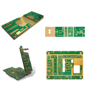
Multilayer HDI PCB Board Application
Substrate and Interposer technology is used for flip-chip or wire-bondable substrates. Microvias offer the escape for very dense flip-chip area arrays. Dielectric is new-engineered films.
A typical example is seen in below Figure. in the subsequent we will discuss these substrates in more detail.[/vc_column_text][/vc_column][/vc_row]
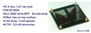
Flip-chip substrate for a memory BGA
Modules are small substrates that may have their ICs wire bonded, flip-chipped, or TAB mounted or may use fine-pitch CSPs. The discrete components are typically very small, such as 0201s or 0101s, and may even be embedded. The design rules are usually coarser than the single IC substrate, since the module may be larger than a single IC package. A typical
example is seen in below Figure.
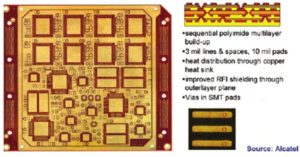
High-performance system module for the base-station for video encryption


