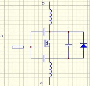
Because the Mosfet Drive Circuit Layout Design will have parasitic inductance, and the parasitic inductance and the junction capacitance of the Mosfet will form an LC oscillation circuit.

Mosfet Drive Circuit Layout Design
If the output terminal of the driving chip is directly connected to the gate of the Mosfet tube, then on the rising and falling edges of the PWM wave will generates a lot of vibrations, causing the mosfet to heat up rapidly or even explode. The general solution is to connect a resistor of about 10 ohms in series with the grid to reduce the Q value of the LC oscillator circuit, so that the vibration is quickly attenuated.
Because of the high input impedance of the Mosfet transistor gate, a little bit of static electricity or interference may cause the MOSFET transistor to turn on incorrectly. Therefore, it is recommended to connect a 10K resistor in parallel between the G pole and the S pole of the MOS transistor to reduce the input impedance.
If you are worried about the coupling of interference on the nearby power line to produce instantaneous high voltage breakdown MOS tube, you can connect a TVS transient suppression diode of about 18V in parallel between GS.
TVS can be regarded as a voltage regulator tube with a fast response speed, which can withstand power up to several hundred to thousands of watts in an instant, which can be used to absorb instant interference pulses.


