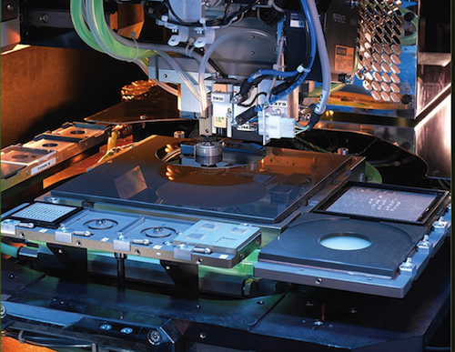
Lithography processing technology refers to the key process technology of processing semiconductor structure and integrated circuit micro-graphic structure, and it is a kind of micromanufacturing technology which is applied earlier and is still widely used in the field of micromanufacturing.

The principle of lithography is similar to photographic plates in printing technology, applying photoresists to silicon (Si) semiconductor substrate materials, and then exposing the photoresist layer by mask, etc., and obtaining the same very fine geometry of the anti-etching layer in the corrosion inhibitor layer. Microstructures are created on the substrate.
The process of lithography technology is
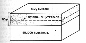
1) Oxidation. Create siO2 oxidation layer on the surface of the Si wafer.

2) Apply glue. Apply a layer of photoresist to the surface of the SiO2 oxide layer, with a thickness of 1 to 5 pm.
3) Exposure. Place the mask at the level of the corrosion inhibitor, and then use ultraviolet light and other methods to combat the exposure of the corrosion agent.
4) Development. The exposed corrosion inhibitor is removed by the developer solution, and the processing graph is displayed.
5) Etching. Using chemical or physical methods, siO, which is free of photoresistor sits, is corroded off, and is called etching.
6) Deglue. After etching, the photoresistr completes its due effect and tries to remove it.
7) Diffusion. Depending on the need, impurities can be further diffused to the parts where impurities are in need to enhance the performance of the microcomponents.


