After the completion of Printed circuit board schematic diagram, designer will start to Layout PCB Board from Schematic Diagram.
In the Package Library, the package of one component includes both the schematic package and the PCB package. The figure below is the component package library of Altium Designer software. In the package library named component_library, the part with the suffix SchLib is its schematic package library, and the suffix for PchLib is the PCB package library.
That is to say, the illustration we draw in the schematic diagram also needs the corresponding PCB package to be a complete package (the drawing of the PCB package is not mentioned here). The schematic package and the PCB package are one-to-one, so that we can use the software to export PCB files from the schematic.
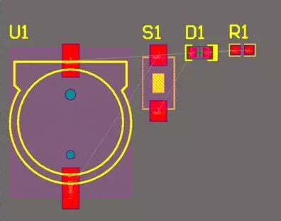
The exported PCB file will disturb the arrangement of the various components. Just like in the physics lab class, we push all the connected circuit devices into a row along the wall. We export the schematic that has just been drawn:

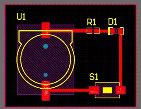
Then we need to layout the components, which is equivalent to putting the component back neatly back on the table. It should be noted that the thin yellow line on the graph does not mean that the components are connected, but the software reminds you that this is the wiring part of the schematic diagram. We also need to manually pull the wires according to the thin yellow line. The following figure shows the PCB layout of a simple layouting and wiring.

A few red rectangles are the pad portion of the PCB, which is the part where the component’s pins are in contact with the PCB. The components are connected by a red line. In a real PCB board, the red part is the area where the copper is located. We solder the components to the board, and the pads and red lines are connected together to form a path which can be called circuitry pattern which is a necessary part for PCB board reverse engineering.
We sent above Figure to the PCB manufacturer to produce the real PCB board, and then soldered the various components, a beautiful PCB is completed.


