
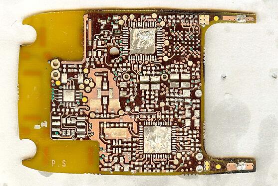
The basis for any PCB board reverse engineering is to first identify the digital image of the pads, holes, tracks, vias, and copper tracks on the PCB and this process has been refered as Image processing and Recognition. Digital image extraction of the PCB can be performed using computer image processing techniques and then identified.
The PCB board Reverse Engineering is based on the analysis and processing of non-electrical measurement technology software. The PCB is imaged and digitized by a graphic input device to generate a bmp format graphic file of the PCB.
The objects recognized by the board image include through holes, half holes, and lines on the board.
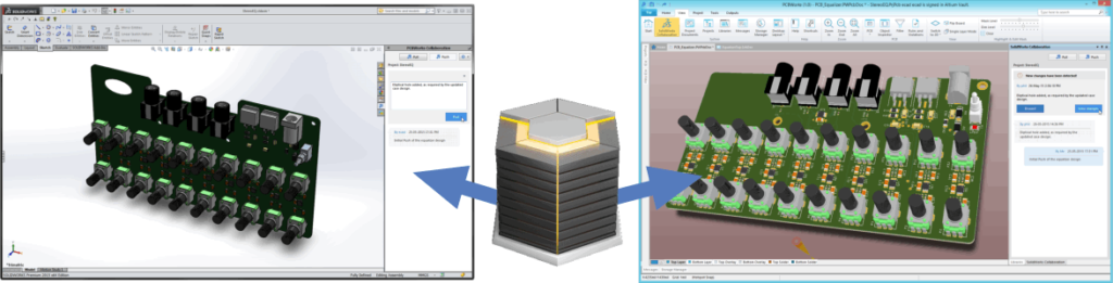
Non-contact circuit board reverse engineering image processing and automatic identification system is the first step in the whole pcb reverse engineering system. Its success can directly affect the efficiency of the reverse engineering PCB board process and may even affect the success or failure of the whole reverse engineering process.
It takes the three-color (red, black, blue) bitmap file processed by the image processing software as input, and outputs the coordinates of the points and lines after recognition. The image recognition system is divided into three parts.
Points: image acquisition section, image processing section, image recognition section. It is found that the basic functions required for the non-contact printed circuit board reverse engineering image processing part include image weight graying, binarization, image rotation, image refinement and median filtering.


