Reverse Engineering printed circuit board will help to engineer to recover original PCB layout diagram from physical sample, so how to Improve PCB Board Layout Design Drawing Cloning Quality become an inevitable subject for discussion:
Most of the time, the circuitry diagrams and designs that appear in textbooks are very different from the actual printed circuit board design that we complete in our daily work. Circuit layout design is not easy, because it requires a full understanding of each component that makes up the circuit part, and a lot of practice is needed to achieve a “perfect” design. However, when you keep in mind and apply the following skills in circuit design, they will help make your circuit look more professional, work at the best efficiency, and improve your professionalism.
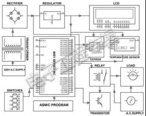
One of the method we can use is using block diagram

How to Improve PCB Board Layout Design Drawing Cloning Quality

This technique seems obvious, but it is often overlooked by overconfident people who think they have already figured out all the work to be done. A reversed pcb board diagram that describes the circuit exactly according to your needs is critical to the successful design of the circuit. Before you start working, the block diagram provides you with an outline. It also provides an excellent reference for anyone who will look at and inspect your circuit.
In many cases, you may not work alone when reverse engineering a circuit board’s gerber file, so take the time to divide the design into functional blocks, each block has a defined interface, and you can realize each breaking strategy; participate in the cloning of the circuit board’s design,
The teacher can focus on each block. These blocks can be used independently for the project you are currently working on, or they can be reused for different circuit designs in the future. In this way, you can easily troubleshoot when things are not going well, because you will be able to identify which part of the trouble you are having caused.


