In practical engineering applications, EDA (Electronic design automation) drawing tools are required to Draw PCB Board Schematic Diagrams. The schematic drawing software commonly used by engineers is PADS, OrCAD, Altium Designer (Protel) and so on. Although the positioning of several softwares is different, they are basically the same in the process of drawing schematic diagrams
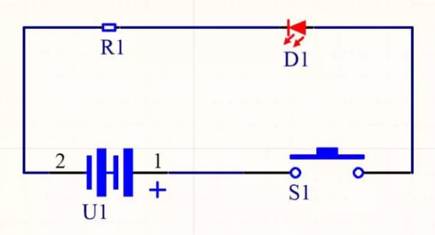
Below, I use Altium Designer software to demonstrate the drawing flow of the schematic diagram of below Figure. Simply put, draw a component, connect them together, and then move the circuitry pattern to the PCB board.

Drawing the PCB Board schematic diagram package
To draw a schematic, first draw the schematic package, which is to draw an abstract icon for each component,
Let’s take the resistor component of above figure as an example to draw its schematic package. The rectangle we have surrounded by four blue lines represents the resistance. Since the resistor has two ends, we add 2 pins to the resistor and place them on both ends of the blue rectangle. The schematic package of such a resistor is done.
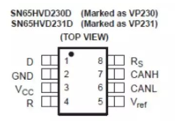
As for Light-emitting diodes, switches, and batteries are drawn in the same way as a simple graphic and pin combination, so how do you draw a schematic package of a more widely used integrated circuits? Taking Texas Instrument’s CAN transceiver chip SN65HVD230 as an example, we first find the data-sheet of this chip (datasheet, which can be found on the chip manufacturer’s official website and critical when draw the schematic diagram for PCB reverse engineering), and then find its pin function part, which is shown in the figure below. Obviously this chip has 8 pins (see below figure):

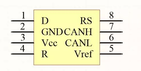
Then, according to the description of the pins in the data sheet, we add 8 pins to this rectangle, and the PCB Board schematic diagram package of one integrated circuit with SOP-8 is done:

The name and serial number of the pin must be strictly in accordance with the data sheet. If the error is drawn, the chip pin connection in the PCB board will be wrong. We can’t waste the package of the painting, we usually put them one by one into an integrated circuit library, and take it out next time, without having to paint again.
In fact, to draw a diagram of components, we only need to pay attention to the name and configuration of the pin, without paying too much attention to the color shape of the figure, etc., because this illustration only represents the electrical properties of the chip.


