One of the purpose of PCB Board Reverse engineering is to restore its schematic diagram, how to draw a good Schematic Diagram of PCB Board Reverse Engineering is a main subject for the engineer, Not only the code is readable, but also the schematics. In many cases, the schematic diagram is not only for yourself, but also for others. If the readability is poor, it will cause a series of communication problems. Therefore, it is necessary to develop good habits and make a standardized schematic diagram. In addition, an excellent schematic diagram will also consider testability, maintainability, BOM normalization, etc.
First of all, separate the block according to the functions:

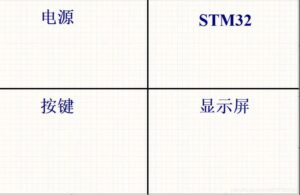
separate functional blocks of PCB board reverse engineering
Use lines to divide the entire schematic diagram into areas, and write functional descriptions for each area, such as: power supply, STM32, etc. This allows people to understand the entire schematic diagram more clearly and quickly, and it is also easy to find the circuit pattern based on the problem when debugging and reverse engineering circuit board.
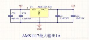
The critical parameters must be specified clearly when draw schematic diagram of PCB board reverse engineering;

The critical parameters must be specified clearly when draw schematic diagram of PCB board reverse engineering;
As shown in the figure above, the maximum output current is marked, so that it is convenient for others to know whether the power supply can carry the load when redesigning the circuit board layout drawing. You can also write other parameters, such as: input voltage range, applicable temperature range, and even truth table in digital circuits, etc.


