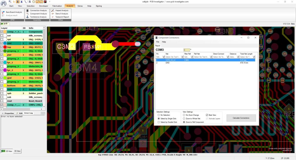
Hereby we would like to discuss how to design Component in PCB Board Cloning through the standard procedures to get a complete and functional drawing:

“Component placement” is the most important function of component pin connection processing. The component arrangement is divided into two-pins component arrangement, three-pins component arrangement, chip arrangement, switch socket arrangement and small three-pins, small four-pins component arrangement in the process of circuit board cloning.
When the component is arranged, the description of the component is drawn, and the component pins and the connected pads are automatically wired.
“Component property setting” is related information such as component identification, component packaging, etc., which are related to the component after completing the connection between the component’s pin and the solder joint. This information is used to generate a netlist in PCB clone service and analyze the connection between component pins.
“Parallel movement” is mainly a function set for the position of the solder joint arrangement. In the process of image recognition solder joints or manual placement of solder joints in the image of the PCB board, it is inevitable that the position of the arrangement is too different from the original position. In this case, the solder joint is required to be adjusted.
Copy, undo and then redo, etc. are auxiliary functions for the above operations to improve operational efficiency.


