The Gerber File format is an open 2D binary vector image file format. It is the standard file used by printed circuit board (PCB) industry software to describe the printed circuit board images: copper layers, solder mask, legend, etc. Designer can use this documents and send it to manufacturer for Printed circuit board production, normally this file can be converted from Layout drawing which can be opened and viewed by PADs2005, hereby we would like to introduce the way to convert PADs2005 to PCB Gerber file:
*.PCB, The file with PCB suffix can be opened by double-clicking the file directly. You can also open the PADs2005 and click the toolbar File→Open(Ctrl+O) to open it. The file with the *.asc suffix must be imported by clicking the toolbar File→Import.
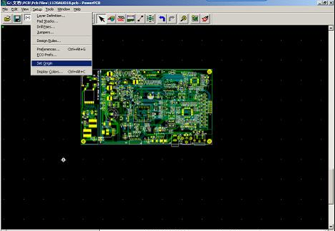
1st step is Press Alt→S→O or select Set Origin in the Setup menu to set the origin to the lower left corner of the graph (you can align the output Gerber file layer with the layer) , see below image:

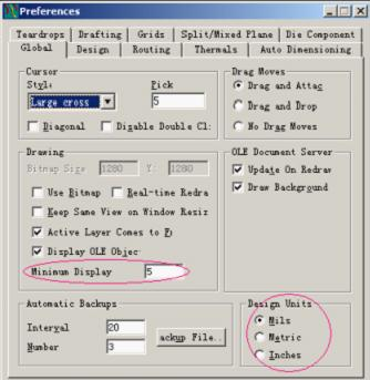
2nd step is Click the toolbar File→Tools→Pour Manager to call up the copper menu in the figure below to select Hatch, Hatch Mode to select Hatch All, press Start to make copper, and press Setup to open Perferences (Ctrl+Alt+G) to system parameters. Some appropriate settings:
Flood: Re-electrically fill all according to the Net-list and Design Rules settings. This item is commonly used for design engineers to layout copper foil on the PCB Board.
Hatch: Filling according to the fill area defined by the customer, that is, turning the copper foil profile seen in the file into a large copper foil. (The circuit board manufacture will use to restore the copper foil plating).
Plane Connect: A special filling area set in the inner layer of the multi-layer PCB board. When the layer property of the multi-layer printed circuit board is the plane dividing surface attribute of the Mix/Splix plane, the Plane Connect is required to fill the copper;
3rd step is to change the unit, Global→Design Units; change the minimum display line width Global→Drawing (in the graphical interface can be set by R+space+value)

the 4th step is Change the fill mesh of the copper skin Global→Design Units, fill direction Drafting→Direction; the value of the Copper in the Hatch Grid is the center-to-center distance of the line filled in the large copper foil.


