
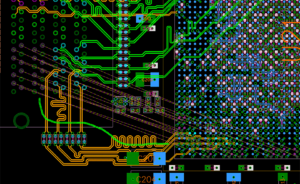
For High Speed Digital Signal PCB Board Reverse Engineering, a 90° corner will have a certain impact on high-speed signal transmission lines. For our current high-density high-speed PCBs, the general trace width is 4-5mil, and the capacitance of a 90° corner is about 10F.
High Speed Digital Signal PCB Board Reverse Engineering
It is estimated that the cumulative delay caused by this capacitance is about 0.25ps, so the 90° corner on the 5mil line width wire will not have a great impact on the current high-speed digital signal circuit board reverse engineering (100-psec rising edge time). For high-frequency signal transmission lines in the PCB board reverse engineering, in order to avoid signal damage caused by the skin effect, a wider signal transmission line is usually used, such as 50Ω impedance and 100mil line width.
The line width at the 90° corner is about 141mil, the signal delay caused by parasitic capacitance is about 25ps. At this time, the 90° corner will have a very serious impact. At the same time, microwave transmission lines always hope to reduce signal loss as much as possible.

high-frequency signal transmission lines in the PCB board reverse engineering
Impedance discontinuities at 90° corners and parasitic capacitance outside will cause phase and amplitude errors of high-frequency signals, mismatches between input and output, and possible Parasitic coupling, in turn, leads to the deterioration of circuit performance and affects the transmission characteristics of PCB circuit signals.


