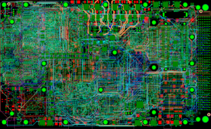
Most people think the BALL GRID ARRAY package with mass chip scale as a feasible solution for portable electronic product to break the space limitation for High Density PCB Board Design.
And it will simultaneously satisfy both the requirement for more complicate functions and performance. However the design high density circuit board of portable electronic product process should take the assembly into account.
When developing electronic products for today’s value-driven markets, performance and reliability are top priorities. In order to compete in this market, developers must also pay attention to the efficiency of assembly because it can control manufacturing costs.
Technological advances and the ever-increasing complexity of electronic products are creating a need for High Density PCB Board Design and fabrication methods. When designing surface-mount, fine-pitch, and vector-packaged integrated circuits, high density printed circuit boards with finer line widths and thinner spacing may be required.

High Density PCB Board Design Global Trend
However, looking to the future, some companies that are already supplying miniature via holes and serially assembled circuit boards are investing heavily to expand their capabilities. These companies recognize the current trend of electronics for smaller packages. The communications and personal computing industry alone is enough to lead the global market.
High Density PCB Board Design is increasingly challenged by several factors: physical, finer pitch pin spacing, in-surfficient financial support, mounting must be very precise, and the environment limitation.
Many plastic packages absorb moisture, causing the crack on assembly processing. Physical factors also include the complexity of the installation process and the reliability of the final product. Further financial decisions must consider how the PCB board will be manufactured and assembled.
More fragile pin components, such as SQFP, shrink quad flat packs with 0.50 and 0.40mm?0.020” and 0.016” pin pitches, may be it will present a challenge to an assembly specialist in maintaining consistent assembly process qualification rate.
The most successful development plans are the PCB board design guidelines and pad geometries that have already undergone process certification.


