Guard Trace in Printed Circuit Board Layout
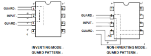
For the left-side inverting mode, note that the Pin 3 connected and grounded Guard Trace in Printed Circuit Board Layout surround the op amp inverting input (Pin 2), and run parallel to the input trace. This guard would be continued out to and around the source and feedback connections of below Figure (or other similar circuit), including an input pad in the case of a cable. In the right-side noninverting mode, the guard voltage is the feedback divider voltage to Pin 2. This corresponds to the inverting input node of the amplifier.

Note that in both of the cases of Below Figure, the guard physical connections shown are only partial—an actual layout would include all sensitive nodes within the circuit. In both the inverting and the noninverting modes using the MINI-DIP or other through hole style package, the PCB guard traces should be located on both sides of the board, with top and bottom traces connected with several vias.

In the case of the follower stage (right), the guard trace must be routed around the negative supply at Pin 4, and thus Pin 4 to Pin 3 leakage isn’t fully guarded. For this reason, a precision high impedance follower stage using an SOIC package op amp isn’t generally recommended, as guarding isn’t possible for dual supply connected devices.
However, an exception to this caveat does apply to the use of a single-supply op amp as a noninverting stage. For example, if the AD8551 is used, Pin 4 becomes ground, and some degree of intrinsic guarding is then established by default.


