

The ground plane from PCB board Layout can act as a shield where sensitive signals cross. Below Figure 12.1 shows a good layout for a data acquisition board where all sensitive areas are isolated from each other and signal paths are kept as short as possible. While real life is rarely as simple as this, the principle remains a valid one.
A engenharia reversa de PCB é o processo de desconstruir e analisar o design e a funcionalidade de uma placa de circuito impresso (PCB) e clonar o layout da placa PCB e o desenho do projeto para copiar 100% perfeitamente as amostras físicas da placa de circuito impresso;
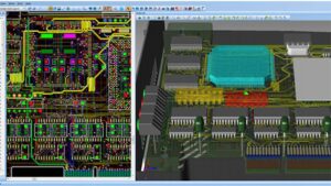
In the process of PCB board Layout, there are a number of important points to be considered when making signal and power connections.
First of all a connector is one of the few places in the system where all signal conductors must run in parallel—it is therefore imperative to separate them with ground pins (creating a Faraday shield) to reduce coupling between them.

الهندسة العكسية لثنائي الفينيل متعدد الكلور هي عملية تفكيك وتحليل تصميم ووظيفة لوحة الدوائر المطبوعة (PCB)، واستنساخ تخطيط لوحة ثنائي الفينيل متعدد الكلور ورسم التصميم لنسخ العينات المادية للوحة الدوائر المطبوعة بشكل مثالي بنسبة 100%؛
Multiple ground pins are important for another reason: they keep down the ground impedance at the junction between the board and the backplane. The contact resistance of a single pin of a PCB connector is quite low (typically on the order of 10 mÙ) when the board is new—as the board gets older the contact resistance is likely to rise, and the board’s performance may be compromised.
It is therefore well worthwhile to allocate extra PCB connector pins so that there are many ground connections (perhaps 30% to 40% of all the pins on the PCB connector should be ground pins). For similar reasons there should be several pins for each power connection.[/vc_column_text][/vc_column][/vc_row]


