Ground Isolation Amplifer in PCB Board Design
Full signal transmission accuracy can still be accomplished in the face of such high noise voltages, by employing a principle discussed earlier. This is the use of a differential-input, ground isolation amplifier. The Ground Isolation Amplifer in PCB Board Design minimizes the effect of ground error voltages between stages by processing the signal in differential fashion, thereby rejecting CM voltages by a substantial margin (typically 60 dB or more).
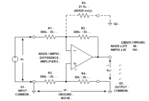
Two ground isolation amplifier solutions are shown in below Figure. This diagram can alternately employ either the AD629 to handle CM voltages up to ±270 V, or the AMP03, which is suitable for CM voltages up to ±20 V.

A Differential Input Ground Isolating Amplifier Allows High Transmission Accuracy by Rejecting Ground Noise Voltage Between Source (G1) and Measurement (G2) Grounds
In the circuit, input voltage VIN is referred to G1, but must be measured with respect to G2. With the use of a high CMR unity-gain difference amplifier, the noise voltage ÄV existing between these two grounds is easily rejected. The AD629 offers a typical CMR of 88 dB, while the AMP03 typically achieves 100 dB. In the AD629, the high CMV rating is done by a combination of high CM attenuation, followed by differential gain, realizing a net differential gain of unity. The AD629 uses the first listed value resistors noted in the figure for R1 to R5. The AMP03 operates as a precision four-resistor differential amplifier, using the 25 kÙ value R1 to R4 resistors noted. Both devices are complete, one package solutions to the ground-isolation amplifier in PCB Board Design.


