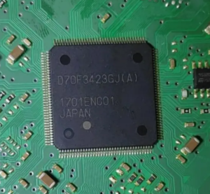
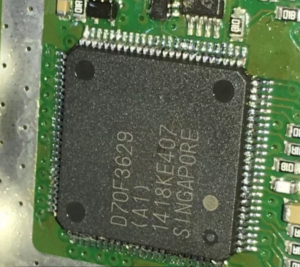
Extract Renesas Locked MCU UPD70F3233M2GK Firmware from its secured flash memory, the protection by its fuse bit of UPD70F3233M2GK microcontroller should be broken, and clone printed circuit board;

Extract Renesas Locked MCU UPD70F3233M2GK Firmware from its secured flash memory, the protection by its fuse bit of UPD70F3233M2GK microcontroller should be broken, and clone printed circuit board;
RTC: Address range 00’ED00h – 00’EDFFh is reserved for the RTC Module access. The RTC is enabled by setting XPEN bit 2 of the SYSCON register and bit 4 of the XPERCON register. Accesses to the RTC Module use demultiplexed addresses and a 16-bit data bus (only word accesses are possible). Two waitstates give an access time of 62.5ns at 64 MHz CPU clock. No tristate waitstate is used.
PWM1: Address range 00’EC00h – 00’ECFFh is reserved for the PWM1 Module access. The PWM1 is enabled by setting XPEN bit 2 of the SYSCON register and bit 6 of the XPERCON register. Accesses to the PWM1 Module use demultiplexed addresses and a 16- bit data bus (only word accesses are possible) to relayout electronic pcb card’s layout and gerber file. Two waitstates give an access time of 62.5ns at 64MHz CPU clock. No tristate waitstate is used. Only word access is allowed.

extrair o firmware MCU UPD70F3233M2GK bloqueado da Renesas de sua memória flash segura, a proteção por seu bit de fusível do microcontrolador UPD70F3233M2GK deve ser quebrada, e clonar a placa de circuito impresso;
ASC1: Address range 00’E900h – 00’E9FFh is reserved for the ASC1 Module access. The ASC1 is enabled by setting XPEN bit 2 of the SYSCON register and bit 7 of the XPERCON register. Accesses to the ASC1 Module use demultiplexed addresses and a 16-bit data bus (only word accesses are possible). Two waitstates give an access time of 62.5 ns at 64 MHz CPU clock. No tristate waitstate is used.
SSC1: Address range 00’E800h – 00’E8FFh is reserved for the SSC1 Module access. The SSC1 is enabled by setting XPEN bit 2 of the SYSCON register and bit 8 of the XPERCON register. Accesses to the SSC1 Module use demultiplexed addresses and a 16-bit data bus. (only word accesses are possible). Two waitstates give an access time of 62.5ns at 64 MHz CPU clock. No tristate waitstate is used.


