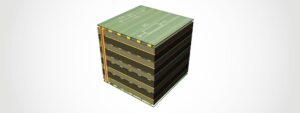
When we clone multi-layer printed circuit board layout diagram, from the original designed PCB stack-up, it can be found that the classic pcb board stack-up design is almost all Even-numbered Printed Circuit Board Layer Structure instead of odd-numbered layers.
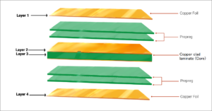
This phenomenon is caused by a variety of factors. It can be known from the manufacturing process of the printed circuit board that all the conductive layers in the circuit board are saved on the core layer. The material of the core layer is generally a double-sided cladding pc board. When the core layer is fully utilized, the number of conductive layer of the printed circuit board is even.

copy multilayer pcb board design file
Even-layer printed circuit boards have cost advantages due to one less layer of dielectric and copper cladding, the cost of raw materials for odd-layer printed circuit boards is slightly lower than that of even-layer printed circuit boards. However, because the odd-numbered layer printed circuit board needs to add a non-standard laminated core layer bonding process on the basis of the core layer structure process, the processing cost of the odd-numbered layer printed circuit board is significantly higher than that of the even-numbered layer printed circuit board.

When we clone multi-layer printed circuit board layout diagram, from the original designed PCB stack-up, it can be found that the classic pcb board stack-up design is almost all Even-numbered Printed Circuit Board Layer Structure instead of odd-numbered layers.
Compared with the ordinary core layer structure, adding copper cladding outside the core layer structure will lead to a decrease in production efficiency and a longer production cycle. The outer core layers require additional processing prior to lamination bonding, which increases the risk of scratching and mis-etching of the outer layers. The added outer layer treatment will substantially increase the pcb board manufacturing cost.


