ESD Suppression on Electronic Board Cloning
When engineer execute Electronic Board Cloning, there will be a criterion on the procedures of ESD suppression, through cloning the layout and gerber file can be extracted and then carry on the re-design to reduce the electronic magnetic static discharge effect on the whole system:
Circuit connection length
A long signal line can also be an antenna that receives ESD pulse energy. Using a shorter signal line as much as possible can reduce the efficiency of the signal line as an ESD electromagnetic field antenna. Try to place the interconnected devices in adjacent locations to reduce the length of the interconnected traces.

ESD Suppression on Electronic Board Cloning
Ground charge injection
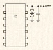
Direct discharge of the ESD to the ground plane may damage sensitive circuitry. One or more high frequency bypass capacitors are used in conjunction with the TVS diodes, which are placed between the power supply of the consumable component and ground. The bypass capacitor reduces charge injection and maintains the voltage difference between the power supply and the ground port.
The TVS shunts the induced current and maintains the potential difference of the TVS clamp voltage. TVS and capacitors should be placed as close as possible to the protected IC (see below Figure), ensuring that the TVS to ground path and capacitor pin length are minimized to reduce parasitic inductance effects.


