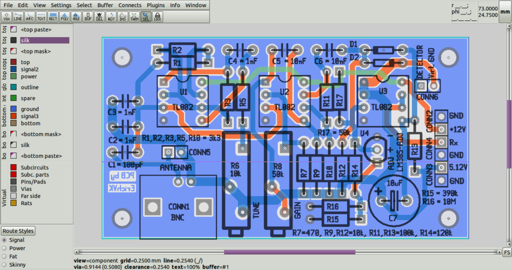
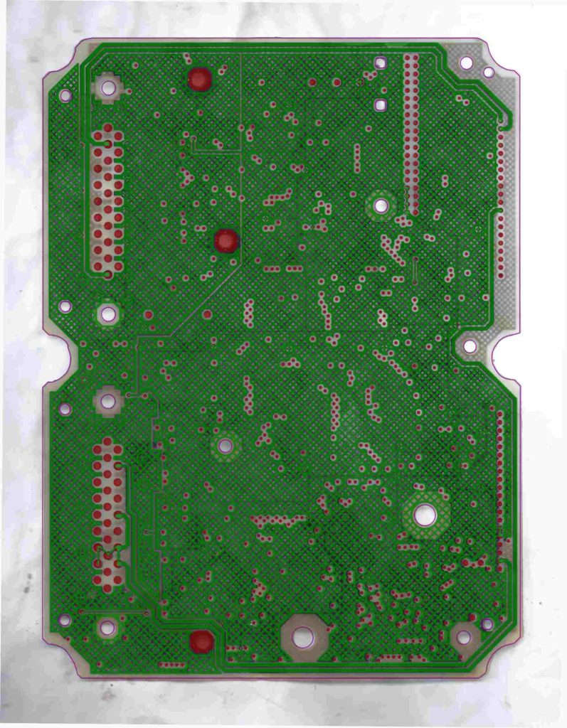
Electronic PCB Circuit Board Rerouting is a process to regenerate original PCB board layout drawing & Gerber file, throught documents the schematic diagram will be restored too;
When Electronic PCB Circuit Board Rerouting, the line directly connected to the pad should not be too wide. The trace should be away from the unconnected components as possible to avoid short circuit; the vias should not be drawn on the components and should be kept away from the unconnected components as much as possible to avoid production phenomenon of virtual welding, continuous welding, short circuit and so on.

In the reverse engineering of RF circuit PCB’s layout and design, the correct wiring of power lines and ground lines is particularly important. Reasonable design is the most important means to overcome electromagnetic interference. A considerable number of interference sources on the PCB are generated by power and ground lines. The noise interference caused by the line is the largest.

The main reason why the ground wire is easy to form electromagnetic interference is that the ground wire has an impedance. When a current flows through the ground wire, a voltage will be generated on the ground wire, thereby generating a ground wire loop current and forming a ground wire loop interference. When multiple circuits share a section of ground, a common impedance coupling is formed, which creates so-called ground noise


