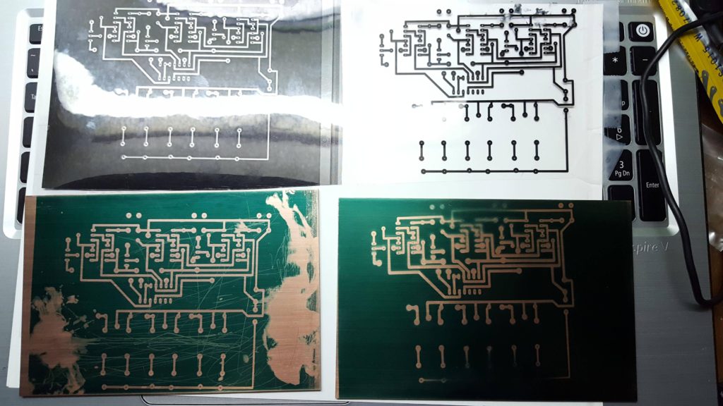
Electronic PCB Circuit Board Conductive Layer can be set either as a signal layer for wiring or as a planar layer for power or ground. In the process of desigining a PCB, the signal layers are called “positive films” and the planar layers are called “negative films”, which differ in design methods. The positive film is empty by default and does not contain any metal conductors. In the design, all the places drawn are required to add metal conductors;

The negative is then full by default and is completely filled with metal conductors. The metal conductors need to be removed wherever they are drawn. The use of the planar layer is not only to solve the power supply and grounding problems of the solder balls in the BGA package chip, but also to shield the electromagnetic interference between the two signal layers.
Because the area that the designer can draw is always smaller than the area that is not drawn, and the area not drawn on the negative is all metal conductors, there are usually large continuous metal conductors on the planar layer.
At the same time, the metal conductor has the function of shielding electromagnetic waves, so placing a planar layer between each two signal layers can effectively reduce electromagnetic interference between the two signal layers. In summary, in the laminated design of the multilayer printed circuit board, the signal layer and the planar layer should generally be alternately placed to ensure at least one planar layer between each two signal layers.


