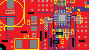
Electronic PCB Board Design Layout Cloning can choose automatic circuitry re-routing, manual rerouting pcb board layout design is an important process of printed circuit board reverse engineering now and in the future.

Electronic PCB Board Design Layout Cloning can choose automatic circuitry re-routing, manual rerouting pcb board layout design is an important process of printed circuit board reverse engineering now and in the future.
Using manual wiring helps automatic wiring tools to complete the wiring work, regardless of the number of key signals, these signals should be routed first, either manually or in combination with automatic routing tools. Critical signals usually must be carefully designed to achieve the desired performance.
After the wiring is completed, the relevant engineering personnel will check the signal gerber layer rerouting result, this process is relatively easy, after passing the inspection, fix these lines, and then start automatic wiring of the remaining signals.
The wiring of key signals needs to consider controlling some electrical parameters during wiring, such as reducing distributed inductance and EMC, etc. The wiring of other signals is similar.
All EDA vendors provide a way to control these parameters. After understanding the input parameters of the automatic wiring tool and the influence of the input parameters on the wiring, the quality of the automatic wiring can be guaranteed to a certain extent.


