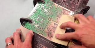
The traditional Electronic Circuit Board Reverse Engineering method is a prototype production method. The reverse engineering flow consists of schematic diagram design, layout and gerber file design, pcb production, measurement and debugging, etc. The disadvantage of this method is that the entire design process is uncontrollable.
In the Electronic Circuit Board schematic diagram and layout drawing design stage, due to the lack of methods and means for effective analysis of the signal transmission characteristics on the actual PCB board, the circuit design can only be based on the recommendations and design experience of component manufacturers and experts. So for a new Electronic Circuit Board Reverse Engineering project, it is often difficult to make the right choice for a specific situation.

In the pcb layout reverse engineering phase, it is also difficult to analyze and evaluate the signal performance changes after layout and routing, so the layout design is more dependent on the designer’s experience. In the board manufacturing stage, due to the different processes of the pcb board and component manufacturers, the parameters of the pcb board and components generally have a large tolerance range, making the board performance more difficult to control.
In the traditional circuit board Reverse Engineering process, the performance of the pcb board is judged only after the completion of the production, and even the problems found in the debugging stage, it must be modified in the next pcb reverse engineering process. But more difficult is that some problems are often difficult to quantify into the parameters of the previous schematic diagram design and layout drawing design, so for more complex pcb boards, it is generally necessary to repeat the above process to meet the PCB reverse engineering requirements.


