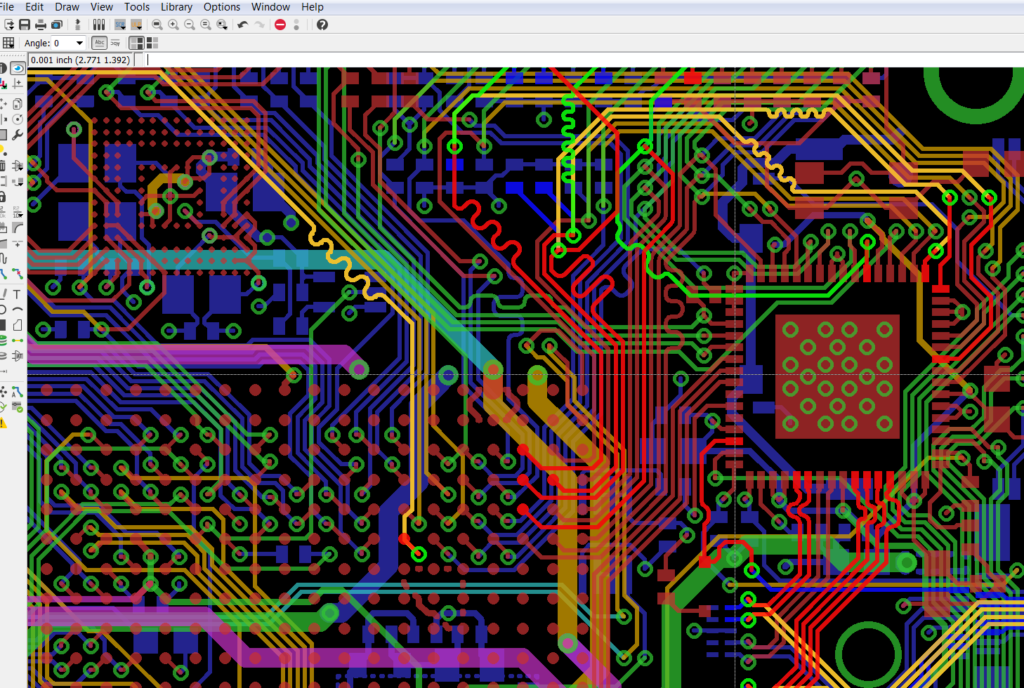
Today’s high-speed system design field has made the traditional pcb design method incompetent. With the rapid development of EDA technology and the corresponding changes in design methods, More and more engineers are adopting electronic board design methods based on signal integrity analysis that are closely integrated with EDA tools.
During the Electronic Board Design process, the designer will devote more time and effort to the constraint definition phase of the pcb board design. Its purpose is to guide the layout and routing of printed circuit board to meet the signal integrity requirements after PCB board manufacturing through perfect design rule constraints.

Through a series of pre-simulations and careful planning of the board topology, it is easy to customize the comprehensive design constraints that meet the required electrical and physical characteristics to avoid the signal integrity issue.
Compared to the traditional pcb design flow, SI-based high-speed PCB design adds pre-simulation and constraint definition definition stages, which not only makes it easier for designers to implement more complex designs, but also achieves controllability of the design process.
In the early stage of layout, problems such as stacking, routing rules, wiring topology, electronic component selection and other factors affecting signal integrity are solved, and there are more design adjustment opportunities to facilitate the improvement of the design scheme.
Post-simulation is a further simulation verification of the actual environment after pcb layouting. Although there may be problems at this stage, the workload of pcb board design modification will be far less than the traditional Electronic Board Design method.
On the basis of the correctness of the SI model and the analytical method, the pcb board can be finalized without requiring or requiring only a few repeated modifications to the design and trial production, thereby shortening the product development cycle and reducing development costs.


