Differential Signal-Handling Technique in PCB Card Design
In general terms, transmitting a signal from one point on a PCB to another for measurement or further processing can be optimized by two key interrelated techniques. These are the use of high impedance, Differential Signal-Handling Technique in PCB Card Design. The high impedance loading of an in-amp minimizes voltage drops, and differential sensing of the remote voltage minimizes sensitivity to ground noise.
This scheme allows relative freedom from tightly controlling ground drop voltages, or running additional and/or larger PCB traces to minimize such error voltages. Note that it can be implemented either with the fixed gain difference amplifiers shown, or also with a standard in-amp IC, configured for unity gain. The AD623, for example, also allows single-supply use. In any case, signal polarity is also controllable, by simple reversal of the difference amplifier inputs.
When the further signal processing is A/D conversion, these transmission criteria can be implemented without adding a differential ground isolation amplifier stage. Simply select an ADC which operates differentially. The high input impedance of the ADC minimizes load sensitivity to the PCB wiring resistance.
In addition, the differential input feature allows the output of the source to be sensed directly at the source output terminals (even if single-ended). The CMR of the ADC then eliminates sensitivity to noise voltages between the ADC and source grounds.
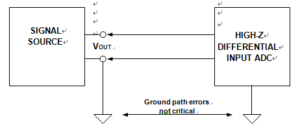
An illustration of this concept using an ADC with high impedance differential inputs is shown in below Figure.

A High-Impedance Differential Input ADC Also Allows High Transmission Accuracy Between Source and Load
Note that the general concept can be extended to virtually any signal source, driving any load. All loads, even single-ended ones, become differential- input by adding an appropriate differential input stage. The differential input can be provided by either a fully developed high Z in-amp, or in many cases it can be a simple subtractor stage op amp.


