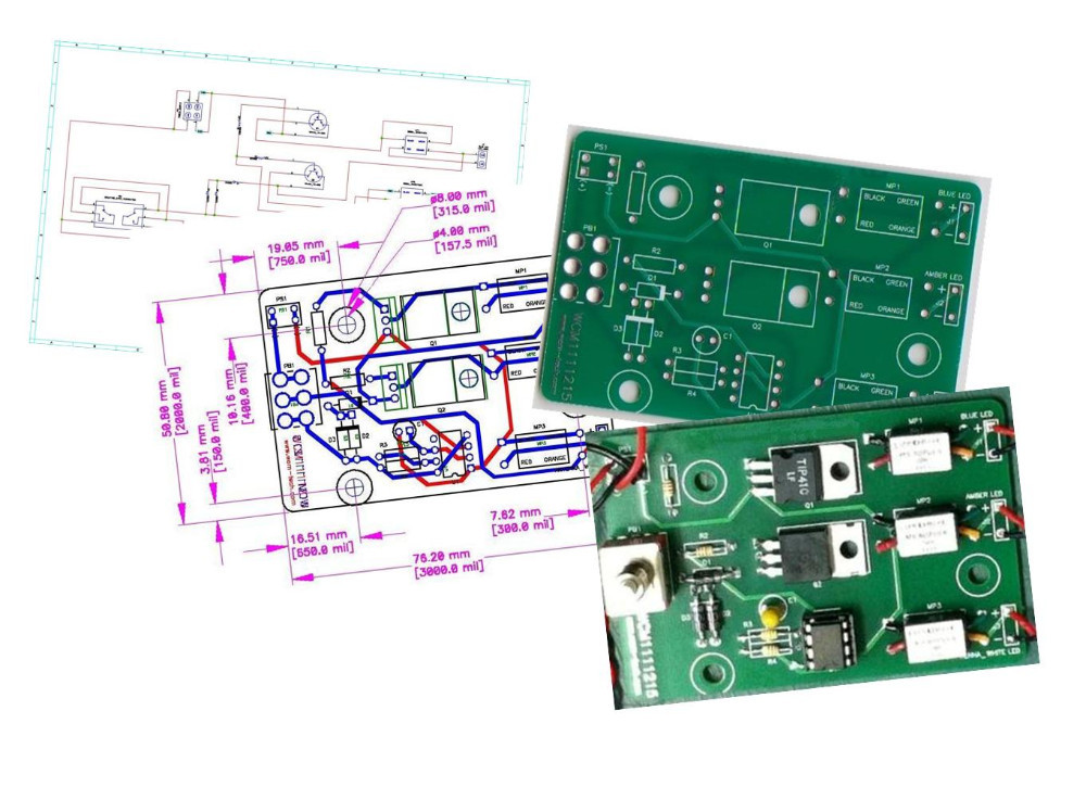
Today let’s talk about the difference between PCB Reverse Engineering and PCB Design,
PCB Board design is just as the name suggests: design the circuit board as required. Circuit board reverse engineering is simply to customize the board according to the provided physical printed circuit board sample.

The circuit board design is mainly because the existing circuit board can not meet the requirements or the product needs to be upgraded, and the new product is developed. The benefits of board design are: it can be distinguished from similar products. It is different from others. Unlimited upgrades are possible during product use.
Many people think that it is the same, but it is still different. The board design can be resized, sized, shaped, and functionally increased or decreased as required to meets the engineer/customer requirements. However, make a PCB cloning is not enough, and it can only be done exactly the same as the one provided. engineer won’t be able to change it at will.
While reverse engineering a circuit board needs to destroy the original circuit board by grinding off the foot of the single integrated chip and reading out the program from Microcontroller flash/eeprom memory which include MCU, CPLD, FPGA etc. The microcontroller may be damaged during the process of hacking. Therefore, it is generally necessary to have 2-3 boards for reverse engineering. In general, 80-90% can be success at one time.


