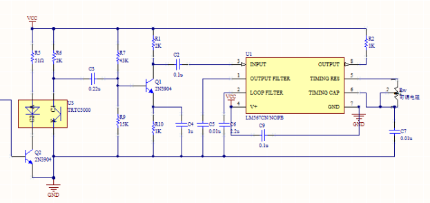
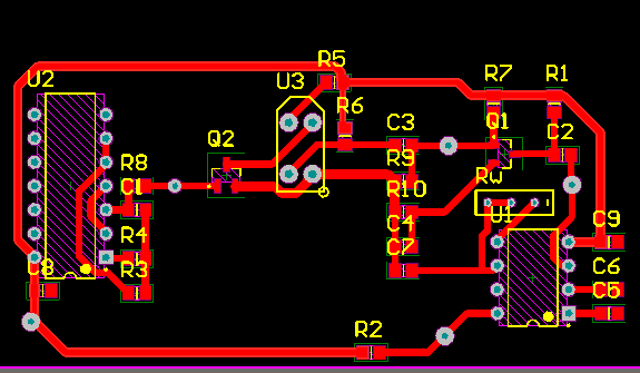
Difference Between PCB Layout and Circuit Board Schematic Diagram are quite obvious, below graphic you can find the Circuit Board Schematic Diagram draw by Altium Designer:

The schematic is used to represent the principle of the circuit board, with some symbols instead of the real components, the following is a layout drawing of the PCB made according to the schematic diagram, which can be regarded as PCB layout, in the PCB reverse engineering, normally we have the schematic diagram from PCB layout and then place the components onto it according to the Bill of material;


