Designing Ground Plane when Reverse Engineering a PCB involves understanding the original board’s layout, identifying ground connections, and following best practices for ground plane design. Here’s a guide on how to approach designing the ground plane during reverse engineering:
-

Designing Ground Plane when Reverse Engineering a PCB involves understanding the original board’s layout,
Identify Ground Connections:
- Schematic Analysis: Refer to the schematic diagram of the PCB to identify all ground connections. Ground symbols, usually depicted as a horizontal bar with multiple triangles pointing downward, indicate where the ground connections are located.
- Physical Inspection: Inspect the actual PCB visually to confirm the ground connections and locate ground pads, traces, and components (such as capacitors connected to ground).
- Ground Plane Purpose:
- Signal Return Path: The ground plane provides a low-impedance return path for signals and helps minimize noise and interference.
- EMI Shielding: A solid ground plane can act as an electromagnetic interference (EMI) shield, reducing the impact of external electromagnetic fields on the circuit.
-

Bir PCB’ye Tersine Mühendislik Yaparken Zemin Düzlemini Tasarlamak, orijinal baskılı devre kartının yerleşim çizimini, gerber dosyasını ve şematik diyagramını anlamayı, toprak bağlantılarını tanımlamayı ve yer düzlemi tasarımı için en iyi uygulamaları takip etmeyi içerir.
Layer Selection:
- Single-Layer PCB: If reverse engineering a single-layer PCB, consider using the copper side as the ground plane and routing traces on the component side.
- Multi-Layer PCB: For multi-layer PCBs, designate one or more internal layers as ground planes. Ensure these layers are dedicated exclusively to the ground and are not shared with signal traces.
- Ground Plane Design Guidelines:
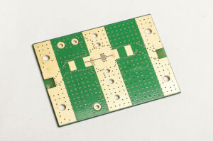
- Continuous Plane: Design the ground plane as a continuous, uninterrupted layer across the designated layer(s) of the PCB. Avoid splitting the ground plane unless necessary for specific reasons.
- Keepout Zones: Define keepout zones to prevent other traces, vias, or components from encroaching on the ground plane area. This helps maintain the integrity and effectiveness of the ground plane.
- Via Placement: Use vias to connect the ground plane on different layers, creating a solid connection throughout the PCB stack-up. Place vias strategically to minimize impedance and ensure a low-resistance path.
- Stitching Vias: Incorporate stitching vias around the perimeter of the ground plane to enhance conductivity and reduce impedance. These vias connect the ground plane to adjacent layers.
- Thermal Relief: Consider using thermal relief pads for through-hole components connected to the ground plane. These pads reduce the heat transfer during soldering, preventing excessive heat from damaging the ground plane.
- Copper Fill: Fill unused areas of the ground plane with copper to maximize conductivity and reduce impedance. This helps maintain a consistent ground reference across the PCB.
- Signal Integrity Considerations:
- Signal Return Paths: Ensure that signal traces have short and direct return paths to the ground plane. Minimize loop areas to reduce inductance and interference.
- Ground Isolation: In sensitive circuits, use ground isolation techniques such as ground splits or star grounding to prevent ground loops and maintain signal integrity.
-

El diseño del plano de tierra cuando se realiza ingeniería inversa en una PCB implica comprender el dibujo de diseño de la placa de circuito impreso original, el archivo Gerber y el diagrama esquemático, identificar las conexiones a tierra y seguir las mejores prácticas para el diseño del plano de tierra.
Simulation and Testing:
- Signal Integrity Simulation: Use PCB design software to simulate signal integrity, ground bounce, and EMI effects on the PCB layout. Adjust the ground plane design as needed based on simulation results.
- Impedance Testing: Conduct impedance testing and continuity checks to verify the effectiveness of the ground plane in providing a low-impedance path.
- Documentation and Revision Control:
- Document Ground Plane Design: Include details of the ground plane design in your PCB documentation, such as layer assignments, via placements, and keepout zones.
- Revision Control: Maintain revision control to track changes to the ground plane design and ensure consistency across iterations of the PCB design.
By following these guidelines and principles, you can design an effective ground plane during the reverse engineering of a PCB, helping to optimize signal integrity, reduce noise, and enhance the overall performance of the circuit.

Progettare il piano di terra durante il reverse engineering di un PCB implica comprendere il disegno del layout del circuito stampato originale, il file Gerber e il diagramma schematico, identificare le connessioni di terra e seguire le migliori pratiche per la progettazione del piano di terra.


