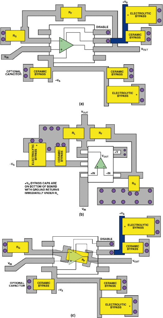
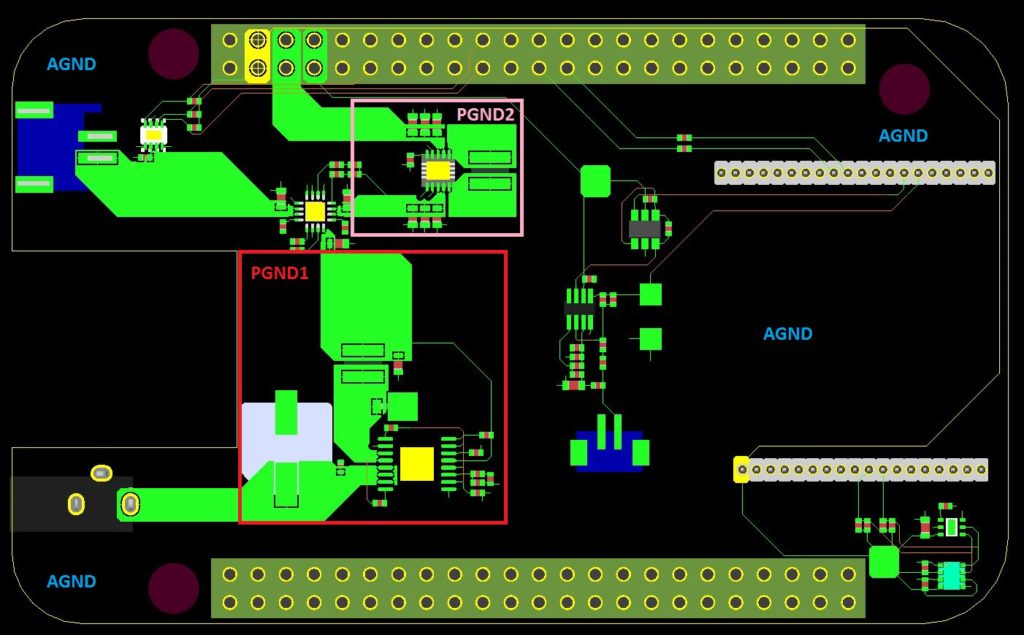
Design PCB Analog/Digital Circuit starts from dividing its structure into four types of circuits (RF analog signals, interface circuits, common digital circuits, -48V, power supply and other high-power wiring areas) to reduce mutual interference between various types of circuits and improve resistance to interference outside the equipment and reduce external emissions.
The long-distance reset line of the circuit board must be connected to a bypass small capacitor at the input pin.
The printed circuit board layout should be avoided to place the electrostatic sensitive device (electrostatic damage threshold less than 2000VHBM) interference source circuit within 20mm from the plug handle panel.
Pull-up pull-down resistors and RC networks that are impedance matched to the transmission line should be as close as possible to the receiver position
The layout of the high-frequency / high-speed circuit board and the sensitive circuit is as compact as possible, minimizing the sensitive signal loop area, and away from other high-frequency high-speed circuits and sensitive circuits

High-speed circuits and sensitive circuits should be kept away from the edge of the PCB as much as possible, and the minimum is not less than 2.5mm, as much as 5mm.
The layout between the high-speed circuit and the sensitive circuit is as isolated as possible. When the resources are limited, the interference source should be given priority. The single-ended clock circuit above 10MHz, some boards do not have weak RF or analog circuits. Think of a strong interference circuit as a sensitive circuit
If there is a small number of signal lines associated between the digital circuit of the partition and the analog circuit, it should be bridged between its separated digital ground and analog ground.

High current devices should be placed as close as possible to their power supply, away from the I/O circuit area


