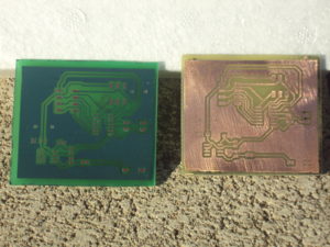
The first step of Copy Printed Circuit Board Gerber File is to get a PCB.
Record the model, parameters, and position of all the components on the paper, especially the direction of the diode, the three tubes, and the direction of the IC notch. It is best to take a photo of two positions with a digital camera.
In the second step, all devices are removed and the tin in the PAD hole is removed. Clean the PCB with alcohol, then put it into the scanner, start POHTOSHOP, scan the silk-screen surface in color, and print it out for use.
In the third step, the TOP LAYER and BOTTOM LAYER layers are slightly polished with water-dyed paper, polished to a copper film, placed in a scanner, and the PHOTOSHOP is activated, and the two layers are separately scanned in color. Note that the PCB must be placed horizontally in the scanner, otherwise the scanned image will not be used.
The fourth step of Copy Printed Circuit Board Gerber File is to adjust the contrast and brightness of the canvas so that the portion with the copper film and the portion without the copper film are strongly contrasted, then turn the secondary image to black and white to check whether the line is clear. If it is not clear, repeat this step. If it is clear, save the picture as black and white BMP format files TOP.BMP and BOT.BMP.
The fifth step is to convert the two BMP files into PROTEL format files, and transfer them into two layers in PROTEL. If the two layers of PAD and VIA are basically coincident, it indicates that the first few steps are very good. If there is a deviation, repeat the third step.
Sixth, will be TOP. BMP is converted to TOP. PCB, pay attention to the layer of SILK, which is the yellow layer, then you can trace the line in the TOP layer, and place the device according to the drawing in the second step. Remove the SILK layer after painting.
The seventh step will be BOT. BMP is converted to BOT. PCB, pay attention to transform to the SILK layer, which is the yellow layer, then you can trace the line on the BOT layer. Remove the SILK layer after painting.
The eighth step is to TOP in PROTEL. PCB and BOT. PCB transfer, combined into a picture is OK.
The last step of Copy Printed Circuit Board Gerber File, the TOP LAYER and BOTTOM LAYER are printed on the transparencies (1:1 ratio) with a laser printer, and the film is placed on the PCB to compare whether there is any error. If it is correct, you are done.


