Copy Multilayer PCB Board Layer
The process of Copy Multilayer PCB Board started from removing all of the components off the board and make sure the surface is clean without any solder tin residue. There are several steps to be followed:
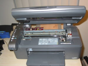
1, Scan the top layer of Multilayer PCB board, save the picture, named as top.jpg, then set the scan DPI, this parameter can be set according to the density of PCB Board, density is a value which is determined by the quantity of holes, pads and nodes, let’s presume the setting is 400DPI.
2, Scan the bottom layer, save the picture, the name as bottom.jpg

scanning pcb pictures
3, Expose Internal layer copper circuitry pattern with coarse sandpaper, make sure the layer has been clean, and then scan the picture and name as mid1.jpg
4,Grind out the middle layer 2 with coarse sandpaper, ensure the copper circuitry pattern has been fully exposed, clean it and scan the picture. Name the image as mid2.jpg;
5, Open PHOTOSHOP editing software to adjust the orientation of each picture (rotate pictures, to ensure that the picture is level, so that the tracks can be viewed in a better perspective, and easier to align the images from top to bottom layer),
Normally the bottom layer image will be made as a horizontal mirror, so when engineer view from top to bottom, all of the positioning holes can be aligned properly.

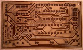
lay up the PCB image and make the drawing
Finally save each picture as BMP format, such as: top.bmp, bottom.bmp, mid1.bmp, mid2.bmp, mid3.bmp, etc
Please remember there is no need to trim the picture too close to the real edge but leave some space on the profile.


