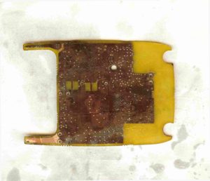
Copy Electronic Circuit Board CAD File is a process to transfer the circuitry pattern of PCB board from scanned pictures to the real CAD file, this part will copy the board according to below Figure, the specific operations are as follows:

Copy Electronic Circuit Board CAD File is a process to transfer the circuitry pattern of PCB board from scanned pictures to the real CAD file
(1) Open the reverse engineering printed circuit board software, the PCB board copying software used in this example is Quick-Pcb (multilayer pcb board can be copied, the line width is greater than 0mil), click on the file \ open the base map \ select the file
(2) According to the data provided by the pcb reverse engineering data collection part, operate on the top of Figure 3-d in the order of pads, vias, wires, and copper surfaces. When adding objects, the position accuracy of the pads and vias should be sufficient Guarantee, there may be some errors in the accuracy of the wire and copper surface.
When connecting the wires, you need to follow the PCB board design rules of the wires, especially the routing mode of the corners of the wires. Generally, 45 degrees is preferred, followed by the arc and the right angle.
When wiring, it is generally necessary to avoid the conductors running at right angles. In principle, the right-angle wiring will cause the line width of the signal line to change, resulting in impedance discontinuity. The impact of right-angle wiring on the signal is as follows: First, right-angle corner wiring is equivalent to the capacitive load of the signal line, which will lead to slower rise time;
The second is due to the discontinuity of the impedance, resulting in signal reflection; the third is that the tip of the right corner should be concentrated force, easy to crack, and EMI will also be generated.


