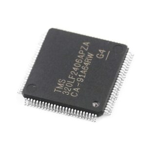
Copy DSP Locked MCU TMS320LF2406AP Flash Code after read TI DSP IC TMS320LF2406AP’s flash memory content, the encrypted microcontroller has been applied on a high density printed circuit board reverse engineering;

Copy DSP Locked MCU TMS320LF2406AP Flash Code after read TI DSP IC TMS320LF2406AP’s flash memory content, the encrypted microcontroller has been applied on a high density printed circuit board reverse engineering
As the XRAM appears like external memory, it cannot be used as system stack or as
register banks. The XRAM is not provided for single bit storage and therefore is not bit addressable.
SFR/ESFR: 1024 bytes (2 x 512 bytes) of address space is reserved for the special function register areas. SFRs are Wordwide registers which are used to control and to monitor the function of the different on-chip units.
CAN1: Address range 00’EF00h – 00’EFFFh is reserved for the CAN1 Module access. The CAN1 is enabled by setting XPEN bit 2 of the SYSCON register and by setting CAN1EN bit 0 of the XPERCON register. Accesses to the CAN Module use demultiplexed addresses and a 16-bit data bus (only word accesses are possible). Two wait states give an access time of 62.5ns at 64 MHz CPU clock. No tri-state wait states are used.

copiar el código flash del MCU TMS320LF2406AP bloqueado DSP después de leer el contenido de la memoria flash de TI DSP IC TMS320LF2406AP, el microcontrolador cifrado se ha aplicado en una ingeniería inversa de placa de circuito impreso de alta densidad;
CAN2: Address range 00’EE00h – 00’EEFFh is reserved for the CAN2 Module access. The CAN2 is enabled by setting XPEN bit 2 of the SYSCON register and by setting CAN2EN bit 1 of the new XPERCON register. Accesses to the CAN Module use demultiplexed addresses and a 16-bit data bus (only word accesses are possible). Two wait states give an access time of 62.5ns at 64 MHz CPU clock. No tri-state wait states are used when reverse engineering circuit board layout schematic.
If one or the two CAN modules are used, Port 4 cannot be programmed to output all eight segment address lines. Thus, only four segment address lines can be used, reducing the external memory space to 5 Mbytes (1 Mbyte per CS line).


