The realization of electronic circuit computer aided design technology can turn schematic diagram into the circuit board, and the PCB reverse engineering techqniue acquire the the schematic diagram, layout drawing, gerber file and bill of material from the printed circuit board, which is a reverse process. There are many problems to be studied in these two technologies, and similar situations exist. Based on the realization of the generalized inversion software, if the interface between the second part and the EDA software routing logic can be realized, the narrow inversion can be realized.

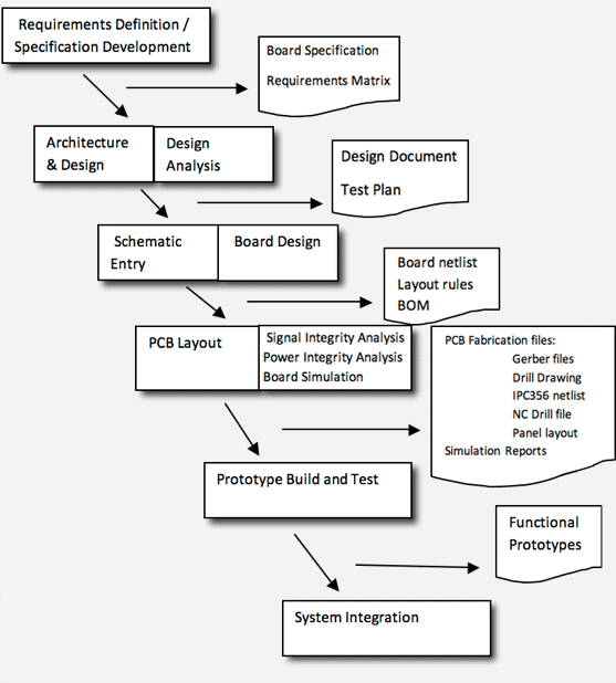
The general flow of circuit board computer aided design technology is shown in below Figure.

This topic is about non-invasive PCB board reverse engineering, and there are many technologies involved. Full invasive circuit board reverse engineering does use scanned images at all, or the images are only used to determine the position of the component. This type of PCB tester is the current type of software. The work done by the software is to automatically draw from the netlist table to the schematic diagram, but the cost of the tester is high and should not be popularized.
Semi-invasive PC board reverse engineering uses digital image and pattern recognition techniques, or a small amount of manual intervention to obtain all the component information and all pin connection information needed to generate a schematic.
Of course, many of the technologies used in practice are integrated. Figure 2.2 reflects various implementation ways of network table source data extraction technology.


